RL78/G1H CHAPTER 18 RF TRANSCEIVER
R01UH0575EJ0120 Rev. 1.20 Page 548 of 920
Dec 22, 2016
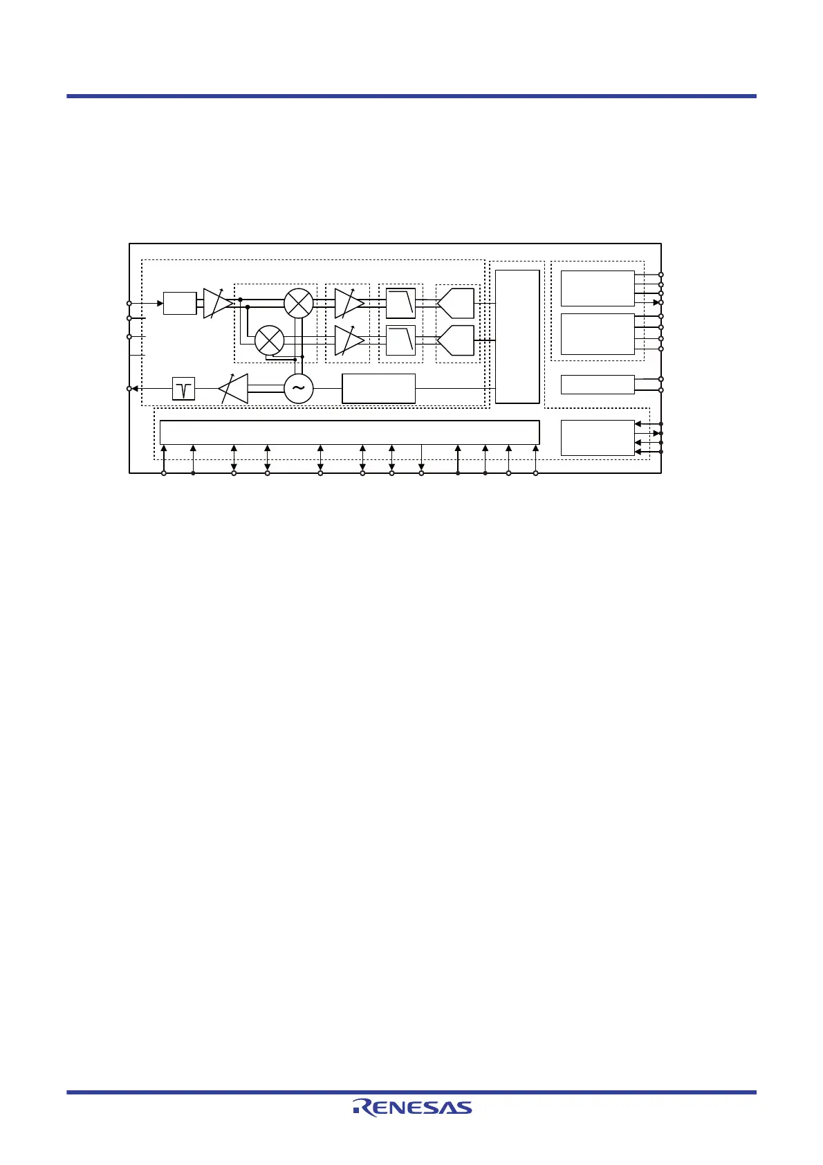
18.3 Configuration of RF Transceiver
RF transceiver consists of the analog block, digital block, power supply circuit block, oscillator block, and interface
block.Figure 18 - 1 shows the block diagram. The next section provides description in detail.
Figure 18 - 1 RF Transceiver Block Diagram
18.3.1 Digital block
(1) Baseband block
For details of the baseband block, see 18.4.
(2) Interface block
This block is equipped with the SPI function for interfacing with MCU.
For details, see 18.5.
(3) Pin control block
Controls I/O, etc. of pins.
SIN
VCCRF
DDCOUT
VCCDDC
SOUT
SCLK
SEN
VSSDDC
Analog block
CONTROL
PLL
ΔΣ Modu la tor
VC O
LPF
MIX
LPF
MIX
PA
RFOUT
VDC
OSC
XIN
XOUT/REFCLKIN
GPIO0/
CLKOUT
REGIN
VREGOUT1
STANDBY
MODE1
VDC
BEF
Internal
Matching
RFIN
RFIP
AGNDRF1
GNDRF2
INTOUT
SPI
DON
RFRESETB
OSCDRVSEL
VREGOUT2
VREGOUT3
GPIO1/
ANTSELOUT0
GPIO2/
ANTSELOUT1
GPIO3 GPIO4/
ANTSW
MODE2
Pin control block
PA block
LNA block
VCO block
PLL block
Filter block ADC blockVGA blockMIX block
Digital block
Base band block
Oscillator block
Interface block
Power supply block
○ Product pin
● Internal pin
 Loading...


