RL78/G1H CHAPTER 3 PIN FUNCTIONS
R01UH0575EJ0120 Rev. 1.20 Page 23 of 920
Dec 22, 2016
3.3 Connection of Unused Pins
Table 3 - 3 shows the Connection of Unused Pins.
Remark For how to handle the ports other than the above, see CHAPTER 5 PORT FUNCTIONS.
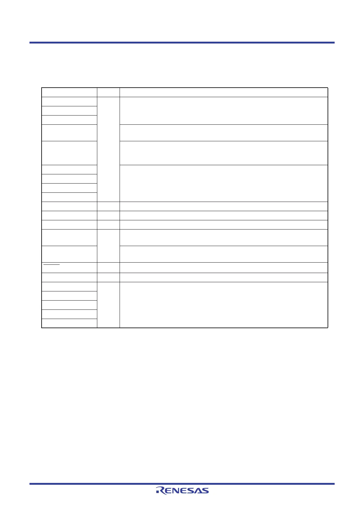
Table 3 - 3 Connection of Unused Pins
Pin Name I/O Recommended Connection of Unused Pins
P02 to P04 I/O Input: Independently connect to V
DD or VSS via a resistor.
Output: Leave open.
P20 to P22
P31
P40/TOOL0 Input: Independently connect to V
DD via a resistor, or leave open.
Output: Leave open.
P60 to P63 Input: Independently connect to V
DD or VSS via a resistor.
Output: Set the port’s output latch to 0 and leave the pins open, or set the port’s output latch to
1 and independently connect the pins to V
DD or VSS via a resistor.
P70 to P72, P75 to P77 Input: Independently connect to V
DD or VSS via a resistor.
Output: Leave open.
P80 to P82
P100
P120
P121 to P124 Input Independently connect to V
DD or VSS via a resistor.
P130 Output Leave open.
P137 Input Independently connect to V
DD or VSS via a resistor.
P140 to P144 I/O Input: Independently connect to V
DD or VSS via a resistor.
Output: Leave open.
P155, P156 Input: Independently connect to V
DD or VSS via a resistor.
Output: Leave open.
RESET
Input Connect to VDD directly or via a resistor.
REGC — Connect to V
SS via a capacitor (0.47 to 1 μF).
GPIO0/CLKOUT I/O Input: Leave open or independently connect to VCCDDC or VSSDDC via a resistor.
Output: Leave open.
GPIO1/ANTSELOUT0
GPIO2/ANTSELOUT1
GPIO3
GPIO4/ANTSW
<R>
 Loading...


