RL78/G15 CHAPTER 1 OUTLINE
R01UH0959EJ0110 Rev.1.10 Page 25 of 765
Mar 7, 2023
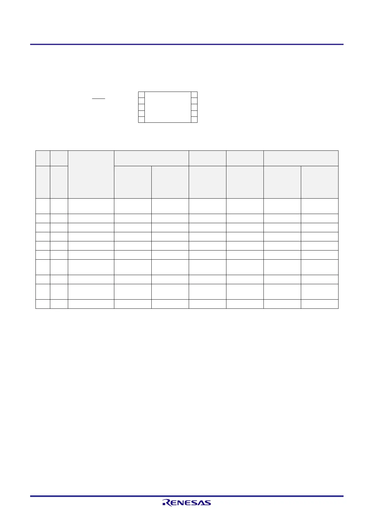
1.3.2 10-pin products
10-pin plastic LSSOP (4.4 × 3.6 mm, 0.65-mm pitch)
1
RL78
/
G15
(Top View)
2
3
4
10
9
8
7
P40/TOOL0/INTP2/(TI01/TO01)/(PCLBUZ
0
)
P125/RESET/INTP1/(VCOUT0)
P137/INTP0/TI00
V
SS
P04
/
ANI3
/IVREF
0
/
INTP
3/TI01
/TO01
P
03/
ANI
2/
INTP4
/
IVCMP0
/TO
00
/SCLA
0/(
TI
00)
P02/PCLBUZ
0/
ANI
1/
INTP7
/
VCOUT0
/SCK
00
/SCL
00
/(TI
01/
TO
01)
P01/TOOLRxD/ANI0/INTP5/TI02/TO02/SI00/RxD0
/SDA
00
/SDAA
0
5
6V
DD
P00/TOOLTxD/INTP6/SO00/TxD0
Table 1-3. Multiplexed Functions of 10-pin Products
Pin
No.
I/O
Power supply,
system, clock,
debug
Analog HMI Timer Communications Interface
10LSSOP
Digital port
A/D converter
Comparator
Interrupt
function
Timer array
unit
Serial array
unit
Serial
interface IICA
1 P40 TOOL0
(PCLBUZ0)
— — INTP2 (TI01/TO01) — —
2 P125 RESET
— (VCOUT0) INTP1 — — —
3 P137 — — — INTP0 TI00 — —
4 — V
SS
— — — — — —
5 — V
DD
— — — — — —
6 P00 TOOLTxD — — INTP6 — SO00/TxD0 —
7 P01 TOOLRxD ANI0 — INTP5 TI02/TO02 SI00/RxD0/
SDA00
SDAA0
8 P02 PCLBUZ0 ANI1 VCOUT0 INTP7 (TI01/TO01) SCK00/SCL00 —
9 P03 — ANI2 IVCMP0 INTP4 (TI00)
TO00
— SCLA0
10 P04 — ANI3 IVREF0 INTP3 TI01/TO01 — —
Remark 1. For pin identification, see 1.4 Pin Identification.
Remark 2. Functions in parentheses can be assigned via settings in the peripheral I/O redirection register (PIOR).
Refer to Figure 4-6 Format of Peripheral I/O Redirection Registers 0 to 3 (PIOR0 to PIOR3).
 Loading...


