RL78/G15 CHAPTER 23 ELECTRICAL SPECIFICATIONS (T
A
= −40 to +85°C)
R01UH0959EJ0110 Rev.1.10 Page 726 of 765
Mar 7, 2023
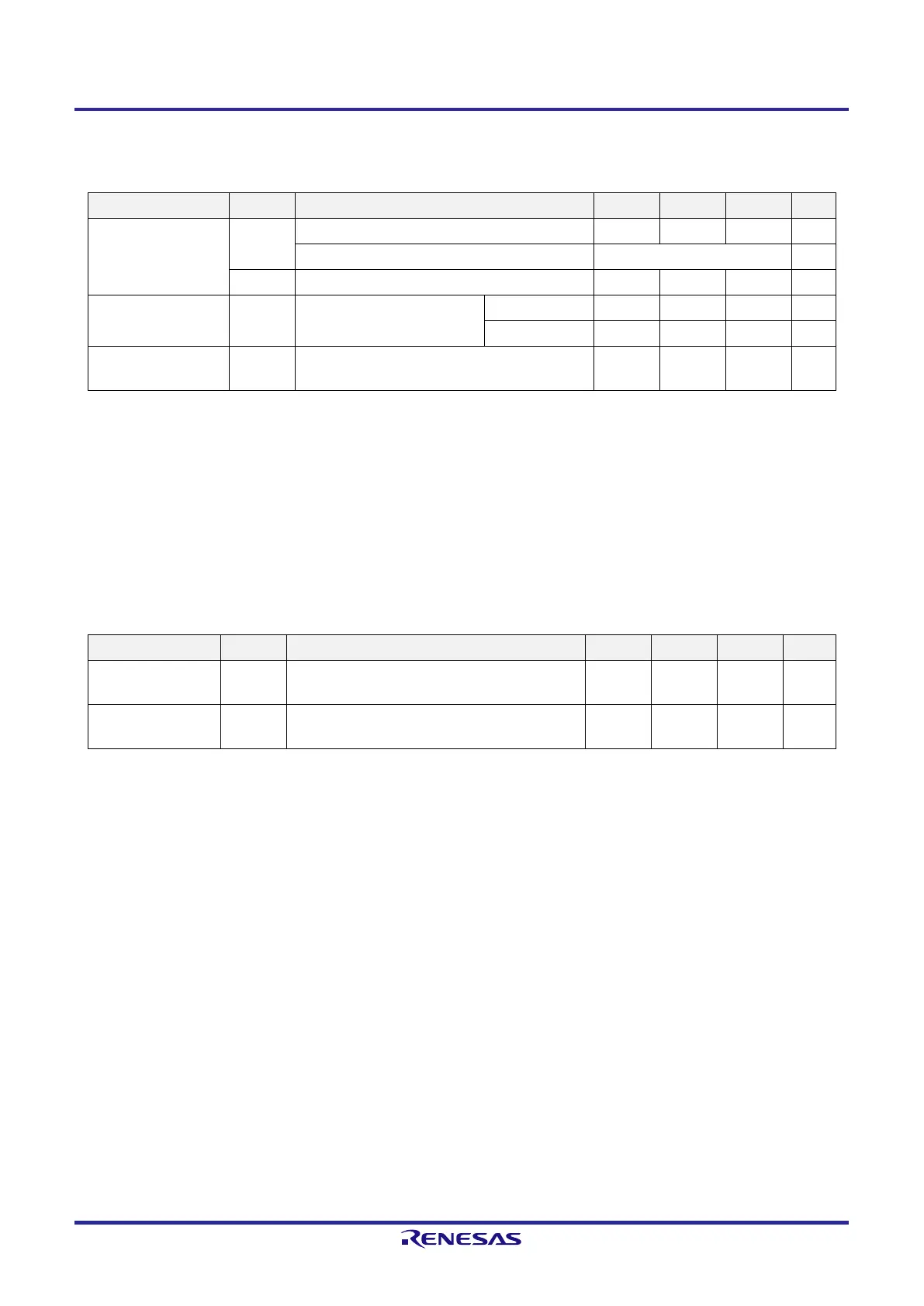
23.6.2 Comparator characteristics
[T
A
= −40 to +85°C, 2.4 V ≤ V
DD
≤ 5.5 V, V
SS
= 0 V]
Item Symbol Condition MIN. TYP. MAX. Unit
Input voltage range I
VREF
IVREFn pin input (CnVRF bit = 0) 0 V
DD
− 1.4 V
Internal reference voltage (CnVRF bit = 1)
Note 1
V
REG
Note 2
V
I
VCMP
IVCMPn pin input −0.3 V
DD
+ 0.3 V
Output delay t
d
V
DD
= 3.0 V,
input slew rate > 50 mV/μs
High-speed mode 0.5 µs
Low-speed mode 2.0 µs
Operation stabilization
wait time
t
CMP
100 µs
Note 1. When the internal reference voltage is selected as the reference voltage of the comparator, the internal
reference voltage cannot be used as the target for A/D conversion.
Note 2. Refer to 23.6.3 Internal reference voltage characteristics.
Remark n: Channel number (n = 0, 1)
23.6.3 Internal reference voltage characteristics
[T
A
= −40 to +85°C, 2.4 V ≤ V
DD
≤ 5.5 V, V
SS
= 0 V]
Item Symbol Condition MIN. TYP. MAX. Unit
Internal reference
voltage
V
REG
0.74 0.815 0.89 V
Operation
stabilization wait time
t
AMP
A/D converter is used (ADS register = 0DH) 5 µs
Caution The internal reference voltage cannot be simultaneously used by the A/D converter and the
comparator; only one of them must be selected.
 Loading...


