RL78/G15 CHAPTER 24 ELECTRICAL SPECIFICATIONS (T
A
= −40 to +105°C, TA = −40 to +125°C)
R01UH0959EJ0110 Rev.1.10 Page 734 of 765
Mar 7, 2023
24.3 DC Characteristics
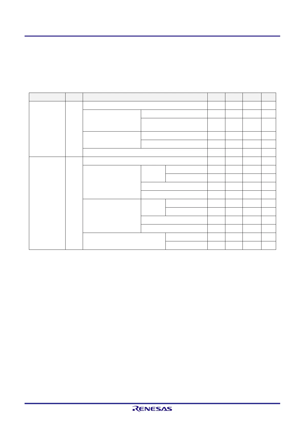
24.3.1 Pin characteristics
[T
A
= −40 to +105°C: G products, T
A
= −40 to +125°C: M products, 2.4 V ≤ V
DD
≤ 5.5 V, V
SS
= 0 V]
(1/2)
Item Symbol Condition MIN. TYP. MAX. Unit
Output current,
high
Note 1
I
OH1
Per pin for P00 to P07, P20 to P23, P40, P41, P121, P122, P125 −3.0
Note 2
mA
Total of P20 to P23, P40,
P41, P121, P122, P125
(when duty ≤ 70%
Note 3
)
4.0 V ≤ V
DD
≤ 5.5 V −25.0 mA
2.4 V ≤ V
DD
< 4.0 V −7.0 mA
Total of P00 to P07
(when duty ≤ 70%
Note 3
)
4.0 V ≤ V
DD
≤ 5.5 V −24.0 mA
2.4 V ≤ V
DD
< 4.0 V −6.0 mA
Total of all pins (when duty ≤ 70%
Note 3
) −40.0 mA
Output current,
low
Note 4
I
OL1
Per pin for P00 to P07, P20 to P23, P40, P41, P121, P122, P125 8.5
Note 2
mA
Total of P20 to P23, P40,
P41, P121, P122, P125
(when duty ≤ 70%
Note 3
)
4.0 V ≤ V
DD
≤ 5.5 V
T
A
= −40 to +105°C 50.0 mA
T
A
= −40 to +125°C 40.0 mA
2.7 V ≤ V
DD
< 4.0 V 10.5 mA
2.4 V ≤ V
DD
< 2.7 V 4.2 mA
Total of P00 to P07
(when duty ≤ 70%
Note 3
)
4.0 V ≤ V
DD
≤ 5.5 V
T
A
= −40 to +105°C 50.0 mA
T
A
= −40 to +125°C 40.0 mA
2.7 V ≤ V
DD
< 4.0 V 9.0 mA
2.4 V ≤ V
DD
< 2.7 V 3.6 mA
Total of all pins (when duty ≤ 70%
Note 3
) T
A
= −40 to +105°C 80.0 mA
T
A
= −40 to +125°C 60.0 mA
Note 1. Device operation is guaranteed at the listed currents even if current is flowing from the V
DD
pin to an output
pin.
Note 2. The value for maximum total current must not be exceeded.
Note 3. The listed currents apply when the duty cycle is no greater than 70%. Use the following formula to calculate
the output current when the duty cycle is greater than 70%, where n is the duty cycle.
Total output current from the listed pins = (I
OH
× 0.7)/(n × 0.01)
Example when n = 80% and I
OH
= –10.0 mA
Total output current from the listed pins = (–10.0 × 0.7)/(80 × 0.01) ≅ –8.7 mA
Total output current from the listed pins = (I
OL
× 0.7)/(n × 0.01)
Example when n = 80% and I
OL
= 10.0 mA
Total output current from the listed pins = (10.0 × 0.7)/(80 × 0.01) ≅ 8.7 mA
Note that the duty cycle has no effect on the current that is allowed to flow into a single pin. A current
higher than the absolute maximum rating must not flow into a single pin.
Note 4. Device operation is guaranteed at the listed currents even if current is flowing from an output pin to the V
SS
pin.
Caution P00, P01, P03 to P07, P22, and P41 do not output high level in N-ch open-drain mode.
 Loading...


