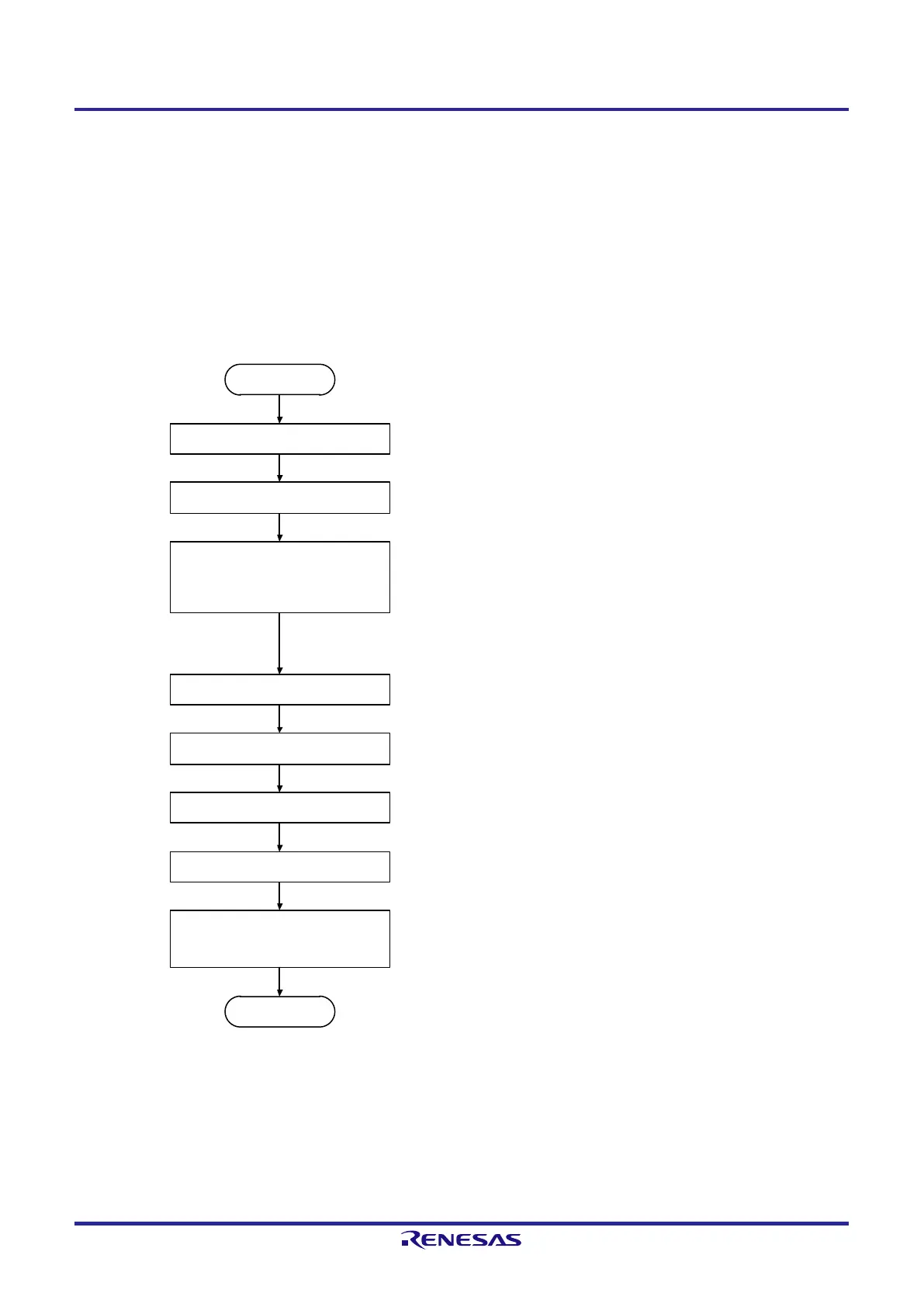
Start of setup
End
Set the PMCx and PMx registers
Set the PER0 register
• Set the ADM0 register
• Set the ADM2 register
• Set the ADS register
(The order of setting is irrelevant.)
Set the ADCE bit
Count the A/D voltage stabilization wait time
Set the ADCS bit
A/D conversion operation
End of A/D conversion
The conversion results are stored in
the ADCR and ADCRH registers
The ADCEN bit of the PER0 register is set (1), and a clock is supplied
to the A/D converter.
The operation of the A/D voltage comparator is started.
• The ADCE bit of the ADM0 register is set (1), and the system enters
the conversion standby state.
After counting of the stabilization wait time ends, the ADCS bit of
the ADM0 register is set (1) and A/D conversion starts.
The ports (ANI0 to ANI10) to be A/D converted are set to analog input.
• Set the bits in the PMCx and PMx registers to 1.
The conversion time and each mode of the A/D converter are set.
• A/D converter mode register 0 (ADM0)
FR1, FR0 and LV0 bits: Select the A/D conversion time.
• A/D converter mode register 2 (ADM2)
ADTYP bit: Select 10-bit or 8-bit resolution.
• Analog input channel specification register (ADS)
ADS3, ADS2, ADS1, and ADS0 bits: Select ANI0 to ANI10
Note 1
as
the target of A/D conversion.
Count the stabilization wait time (0.125 μs) by software.
A/D conversion ends and the conversion results are stored in
the ADCR and ADCRH registers.
At the same time, the A/D conversion end interrupt request signal
(INTAD) is generated, and the ADCS bit of the ADM0 register is
automatically cleared (0) (conversion standby state).
Note 1. ANI0, ANI2, ANI3 for 8-pin products,
 Loading...


