Home
Renesas
Microcontrollers
RL78/G15
Renesas RL78/G15 User Manual
4
of 1
of 1 rating
765 pages
Give review
Manual
Specs
To Next Page
To Next Page
To Previous Page
To Previous Page
Loading...
RL78/G15
CHAPTER 2
5
PAC
KAGE DRAWINGS
R01UH0959EJ011
0
Rev.1
.10
Page
753
of
765
Mar 7, 2023
CHAPTER 25
PACKAGE DRA
WINGS
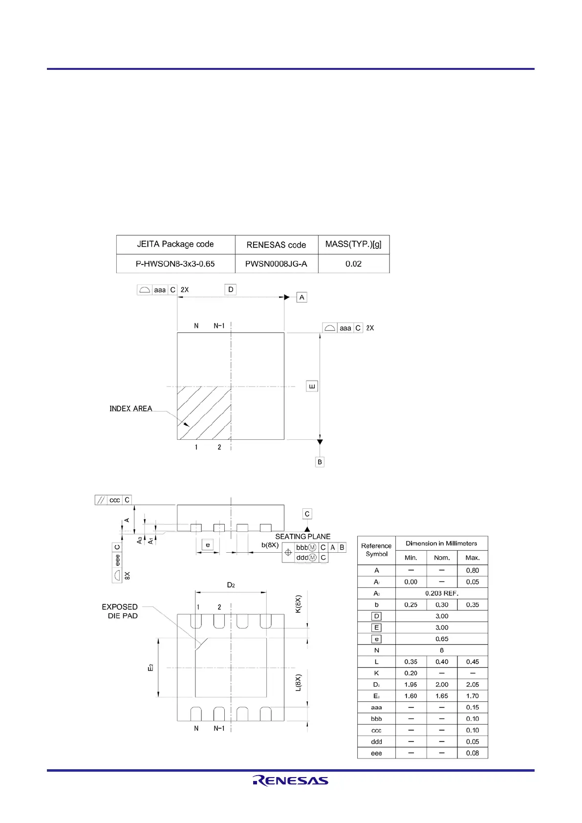
25.1
8
-
pin products
R5F12008MN
S, R5F12008G
NS, R5F12008
ANS
R5F12007MN
S, R5F12007G
NS, R5F12007
ANS
752
754
Table of Contents
default chapter
7
Table of Contents
7
Chapter 1 Outline
19
Features
19
List of Part Numbers
22
Pin Configuration (Top View)
24
8-Pin Products
24
10-Pin Products
25
16-Pin Products
26
20-Pin Products
29
Pin Identification
31
Block Diagram
32
8-Pin Products
32
10-Pin Products
33
16-Pin Products
34
20-Pin Products
35
Outline of Functions
36
Chapter 2 Pin Functions
38
Port Function
38
8-Pin Products
38
10-Pin Products
39
16-Pin Products
40
20-Pin Products
41
Functions Other than Port Pins
43
Functions for each Product
43
Pins for each Product (Pins Other than Port Pins)
44
Connection of Unused Pins
45
Block Diagrams of Pins
46
Chapter 3 Cpu Architecture
55
Overview
55
Memory Space
56
Internal Program Memory Space
59
Mirror Area
62
Internal Data Memory Space
63
Special Function Register (SFR) Area
63
Extended Special Function Register (2Nd SFR: 2Nd Special Function Register) Area
63
Data Memory Addressing
64
Processor Registers
65
Control Registers
65
General-Purpose Registers
68
And CS Registers
69
Special Function Registers (Sfrs)
70
Extended Special Function Registers (2Nd Sfrs: 2Nd Special Function Registers)
73
Instruction Address Addressing
78
Relative Addressing
78
Immediate Addressing
79
Register Indirect Addressing
80
Addressing for Processing Data Addresses
81
Implied Addressing
81
Register Addressing
82
Direct Addressing
83
Short Direct Addressing
84
SFR Addressing
85
Register Indirect Addressing
86
Based Addressing
87
Based Indexed Addressing
91
Stack Addressing
92
Illegal Memory Access Detection Function
95
Chapter 4 Port Functions
97
Port Functions
97
Port Configuration
97
Port 0
98
Port 2
98
Port 4
98
Port 12
99
Port13
100
Registers Controlling Port Function
100
Port Mode Registers 0, 2, 4, 12 (PM0, PM2, PM4, PM12)
103
Port Registers 0, 2, 4, 12, 13 (P0, P2, P4, P12, P13)
105
Pull-Up Resistor Option Registers 0, 2, 4, 12 (PU0, PU2, PU4, PU12)
107
Port Input Mode Registers 0, 2, 4 (POM0, POM2, POM4)
109
Port Mode Control Registers 0, 2 (PMC0, PMC2)
110
Peripheral I/O Redirection Registers 0 to 3 (PIOR0 to PIOR3)
111
Port Function Operations
115
Writing to I/O Port
115
Reading from I/O Port
115
Operations on I/O Port
115
Register Settings When Using Alternate Function
116
Basic Concept When Using Alternate Function
116
Register Settings for Alternate Function Whose Output Function Is Not Used
117
Register Setting Examples for Used Port and Alternate Functions
118
Cautions When Using Port Function
127
Cautions on 1-Bit Manipulation Instruction for Port Register N (Pn)
127
Notes on Specifying the Pin Settings
128
Chapter 5 Clock Generator
129
Functions of Clock Generator
129
Configuration of Clock Generator
131
Registers Controlling Clock Generator
133
Clock Operation Mode Control Register (CMC)
134
System Clock Control Register (CKC)
135
Clock Operation Status Control Register (CSC)
136
Oscillation Stabilization Time Counter Status Register (OSTC)
138
Oscillation Stabilization Time Select Register (OSTS)
140
Peripheral Enable Register 0 (PER0)
142
Operation Speed Mode Control Register (OSMC)
144
High-Speed On-Chip Oscillator Frequency Select Register (HOCODIV)
145
High-Speed On-Chip Oscillator Trimming Register (HIOTRM)
146
System Clock Oscillator
147
X1 Oscillator (16-Pin and 20-Pin Products Only)
147
High-Speed On-Chip Oscillator
150
Low-Speed On-Chip Oscillator
150
Clock Generator Operation
150
Controlling Clock
152
Example of Setting High-Speed On-Chip Oscillator
152
Example of Setting X1 Oscillation Clock
153
CPU Clock Status Transition Diagram
154
Condition before Changing CPU Clock and Processing after Changing CPU Clock
157
Time Required for Switchover of CPU Clock and Main System Clock
158
Conditions before Clock Oscillation Is Stopped
158
Resonator and Oscillator Constants
159
Chapter 6 Timer Array Unit
160
Functions of Timer Array Unit
162
Independent Channel Operation Function
162
Simultaneous Channel Operation Function
165
8-Bit Timer Operation Function (Channels 1 and 3 Only)
167
Configuration of Timer Array Unit
168
Timer Count Register Mn (Tcrmn)
173
Timer Data Register Mn (Tdrmn)
175
Registers Controlling Timer Array Unit
177
Peripheral Enable Register 0 (PER0)
178
Timer Clock Select Register M (Tpsm)
179
Timer Mode Register Mn (Tmrmn)
183
Timer Status Register Mn (Tsrmn)
189
Timer Channel Enable Status Register M (Tem)
190
Timer Channel Start Register M (Tsm)
191
Timer Channel Stop Register M (Ttm)
193
Timer Output Enable Register M (Toem)
194
Timer Output Register M (Tom)
195
Timer Output Level Register M (Tolm)
196
Timer Output Mode Register M (Tomm)
197
Input Switch Control Register (ISC)
198
Noise Filter Enable Registers 1 (NFEN1)
199
Registers Controlling Port Functions of Pins to be Used for Timer I/O
201
Basic Rules of Timer Array Unit
202
Basic Rules of Simultaneous Channel Operation Function
202
Basic Rules of 8-Bit Timer Operation Function (Channels 1 and 3 Only)
204
Operation of Counter
205
Count Clock (F TCLK )
205
Start Timing of Counter
207
Operation of Counter
208
Channel Output (Tomn Pin) Control
213
Tomn Pin Output Circuit Configuration
213
Tomn Pin Output Setting
215
Cautions on Channel Output Operation
216
Collective Manipulation of Tomn Bit
222
Timer Interrupt and Tomn Pin Output at Count Operation Start
224
Timer Input (Timn) Control
225
Timn Input Circuit Configuration
225
Noise Filter
225
Cautions on Channel Input Operation
226
Independent Channel Operation Function of Timer Array Unit
227
Operation as Interval Timer/Square Wave Output
227
Operation as External Event Counter
233
Operation as Frequency Divider (Channels 0 and 3 Only)
238
Operation as Input Pulse Interval Measurement
245
Operation as Input Signal High-/Low-Level Width Measurement
250
Operation as Delay Counter
255
Simultaneous Channel Operation Function of Timer Array Unit
260
Operation as One-Shot Pulse Output Function
260
Operation as PWM Function
270
Operation as Multiple PWM Output Function
279
Operation as Two-Channel Input with One-Shot Pulse Output Function
290
Cautions When Using Timer Array Unit
299
Cautions When Using Timer Output
299
Chapter 7 12-Bit Interval Timer
300
Functions of 12-Bit Interval Timer
300
Configuration of 12-Bit Interval Timer
300
Registers Controlling 12-Bit Interval Timer
301
Peripheral Enable Register 0 (PER0)
301
Operation Speed Mode Control Register (OSMC)
302
Interval Timer Control Register (ITMC)
303
12-Bit Interval Timer Operation
304
12-Bit Interval Timer Operation Timing
304
Start of Count Operation and Re-Enter to HALT/STOP Mode after Returned from HALT/STOP Mode
305
Chapter 8 Clock Output/Buzzer Output Controller
306
Functions of Clock Output/Buzzer Output Controller
306
Configuration of Clock Output/Buzzer Output Controller
307
Registers Controlling Clock Output/Buzzer Output Controller
307
Clock Output Select Register 0 (CKS0)
308
Registers Controlling Port Functions of Clock Output/Buzzer Output Pin
309
Operations of Clock Output/Buzzer Output Controller
310
Operation as Output Pin
310
Chapter 9 Watchdog Timer
311
Functions of Watchdog Timer
311
Configuration of Watchdog Timer
312
Register Controlling Watchdog Timer
313
Watchdog Timer Enable Register (WDTE)
313
Operation of Watchdog Timer
314
Controlling Operation of Watchdog Timer
314
Setting Time of Watchdog Timer
315
Chapter 10 A/D Converter
316
Function of A/D Converter
316
Configuration of A/D Converter
318
Registers Controlling A/D Converter
320
Peripheral Enable Register 0 (PER0)
321
A/D Converter Mode Register 0 (ADM0)
322
A/D Converter Mode Register 2 (ADM2)
326
10-Bit A/D Conversion Result Register (ADCR)
327
8-Bit A/D Conversion Result Register (ADCRH)
328
Analog Input Channel Specification Register (ADS)
329
A/D Test Register (ADTES)
330
Registers Controlling Port Function of Analog Input Pins
330
A/D Converter Conversion Operations
331
Input Voltage and Conversion Results
333
A/D Converter Operation Modes
335
A/D Converter Setup Flowchart
336
Setting up ANI0 to ANI10 for A/D Conversion
336
Setting up the Internal Reference Voltage for A/D Conversion
337
How to Read A/D Converter Characteristics Table
338
Resolution
338
Overall Error
338
Quantization Error
339
Zero-Scale Error
339
Full-Scale Error
339
Integral Linearity Error
339
Differential Linearity Error
340
Conversion Time
341
Sampling Time
341
Notes on A/D Converter
342
Operating Current in STOP Mode
342
Input Voltage on ANI0 to ANI10 Pins
342
Conflicting Operations
342
Noise Countermeasures
342
Analog Input (Anin) Pins
343
Input Impedance of Analog Input (Anin) Pins
344
Interrupt Request Flag (ADIF)
344
Conversion Results Just after A/D Conversion Start
344
A/D Conversion Result Register (ADCR, ADCRH) Read Operation
344
10.9.10 Internal Equivalent Circuit
345
10.9.11 Starting the A/D Converter
345
Chapter 11 Comparator
346
Comparator Functions
346
Comparator Configuration
347
Registers Controlling the Comparator
349
Peripheral Enable Register 0 (PER0)
350
Comparator Mode Setting Register (COMPMDR)
351
Comparator Filter Control Register (COMPFIR)
353
Comparator Output Control Register (COMPOCR)
355
Registers Controlling Port Functions of Comparator I/O Pins
356
Comparator N Operation (N = 0, 1)
357
Comparator N Digital Filter Operation (N = 0, 1)
358
Comparator N Interrupt Operation (N = 0, 1)
358
Comparator N Output (N = 0, 1)
358
Comparator Setting Flowcharts
359
Enabling Comparator Operation (in the Case of CMP0)
360
Disabling Comparator Operation (in the Case of CMP0)
361
Chapter 12 Serial Array Unit
362
Functions of Serial Array Unit
363
Simplified SPI (CSI00, CSI01)
363
Uart (Uart0)
364
Simplified I C (IIC00, IIC01)
365
Configuration of Serial Array Unit
366
Shift Register
368
Lower 8 or 9 Bits of the Serial Data Register Mn (Sdrmn)
369
Registers to Control the Serial Array Unit
371
Peripheral Enable Register 0 (PER0)
372
Serial Clock Select Register M (Spsm)
373
Serial Mode Register Mn (Smrmn)
374
Serial Communication Operation Setting Register Mn (Scrmn)
376
Serial Data Register Mn (Sdrmn)
379
Serial Flag Clear Trigger Register Mn (Sirmn)
381
Serial Status Register Mn (Ssrmn)
382
Serial Channel Start Register M (Ssm)
384
Serial Channel Stop Register M (Stm)
385
Serial Channel Enable Status Register M (Sem)
386
Serial Output Enable Register M (Soem)
387
Serial Output Register M (Som)
388
Serial Output Level Register M (Solm)
389
Input Switch Control Register (ISC)
391
Noise Filter Enable Register 0 (NFEN0)
392
12.3.16 Registers Controlling Port Functions of Serial Input/Output Pins
393
Operation Stop Mode
394
Stopping the Operation by Units
394
Stopping the Operation by Channels
395
Operation of Simplified SPI (CSI00, CSI01) Communication
397
Master Transmission
399
Master Reception
408
Master Transmission/Reception
418
Slave Transmission
428
Slave Reception
437
Slave Transmission/Reception
444
Calculating Transfer Clock Frequency
455
Procedure for Processing Errors that Occurred During Simplified SPI (CSI00, CSI01) Communication
457
Operation of UART (UART0) Communication
458
UART Transmission
460
UART Reception
470
Calculating Baud Rate
477
Procedure for Processing Errors that Occurred During UART (UART0) Communication
482
Operation of Simplified I C (IIC00, IIC01) Communication
483
Address Field Transmission
485
Data Transmission
491
Data Reception
495
Stop Condition Generation
500
Calculating Transfer Rate
501
Procedure for Processing Errors that Occurred During Simplified I
504
C (Iic00, Iic01)
504
Communication
504
Chapter 13 Serial Interface Iica
505
Functions of Serial Interface IICA
505
Configuration of Serial Interface IICA
508
Registers Controlling Serial Interface IICA
512
Peripheral Enable Register 0 (PER0)
513
IICA Control Register 00 (IICCTL00)
514
IICA Status Register 0 (IICS0)
518
IICA Flag Register 0 (IICF0)
521
IICA Control Register 01 (IICCTL01)
523
IICA Low-Level Width Setting Register 0 (IICWL0)
526
IICA High-Level Width Setting Register 0 (IICWH0)
526
Registers Controlling Port Functions of IICA Serial Input/Output Pins
527
I 2 C Bus Mode Functions
528
Pin Configuration
528
Setting Transfer Clock by Using IICWL0 and IICWH0 Registers
529
I 2 C Bus Definitions and Control Methods
531
Start Condition
532
Address
533
Transfer Direction Specification
534
Acknowledge (ACK)
534
Stop Condition
536
Clock Stretching
537
Releasing Clock Stretching
539
Interrupt Request (INTIICA0) Generation Timing and Clock Stretching Control
540
Address Match Detection Method
541
13.5.10 Error Detection
541
13.5.11 Extension Code
542
13.5.12 Arbitration
543
13.5.13 Wakeup Function
545
13.5.14 Communication Reservation
548
13.5.15 Cautions
552
13.5.16 Communication Operations
554
C Interrupt Request (INTIICA0) Generation Timing
564
Timing Charts
585
Chapter 14 Interrupt Functions
600
Interrupt Function Types
600
Interrupt Sources and Configuration
600
Registers Controlling Interrupt Functions
605
Interrupt Request Flag Registers (IF0L, IF0H, IF1L, IF1H)
607
Interrupt Mask Flag Registers (MK0L, MK0H, MK1L, MK1H)
609
Priority Specification Flag Registers (PR00L, PR00H, PR01L, PR01H, PR10L, PR10H, PR11L, PR11H)
610
External Interrupt Rising Edge Enable Register (EGP0), External Interrupt Falling Edge Enable Register (EGN0)
612
Program Status Word (PSW)
613
Interrupt Servicing Operations
614
Maskable Interrupt Request Acknowledgment
614
Software Interrupt Request Acknowledgment
617
Multiple Interrupt Servicing
617
Interrupt Request Pending
622
Chapter 15 Standby Function
624
Overview
624
Registers Controlling Standby Function
625
Standby Function Operation
625
HALT Mode
625
STOP Mode
629
Chapter 16 Reset Function
635
Timing of Reset Operation
637
States of Operation During Reset Periods
639
Register for Confirming Reset Source
641
Reset Control Flag Register (RESF)
641
Chapter 17 Selectable Power-On-Reset Circuit
644
Functions of Selectable Power-On-Reset Circuit
644
Configuration of Selectable Power-On-Reset Circuit
645
Operation of Selectable Power-On-Reset Circuit
646
Cautions for Selectable Power-On-Reset Circuit
647
Chapter 18 Option Byte
648
Functions of Option Bytes
648
User Option Byte (000C0H to 000C2H)
648
On-Chip Debug Option Byte (000C3H)
648
Format of User Option Byte
649
Format of On-Chip Debug Option Byte
652
Setting of Option Byte
653
Chapter 19 Flash Memory
654
Serial Programming Using Flash Memory Programmer
656
Programming Environment
658
Communication Mode
658
Writing to Flash Memory by Using External Device (that Incorporates UART)
660
Programming Environment
660
Communication Mode
661
Connection of Pins on Board
662
P40/TOOL0 Pin
662
RESET ¯¯¯¯¯¯ Pin
663
Port Pins
663
X1 and X2 Pins (16-Pin and 20-Pin Products)
663
Power Supply
664
Serial Programming Method
665
Serial Programming Procedure
665
Flash Memory Programming Mode
666
Selecting Communication Mode
667
Communication Commands
667
Processing Time for each Command When PG-FP5 Is in Use (Reference Values)
668
Self-Programming
669
Registers Controlling Self-Programming
669
Flash Address Pointer Registers H and L (FLAPH, FLAPL)
670
Flash End Address Specification Registers H and L (FLSEDH, FLSEDL)
671
Flash Write Buffer Registers HH, HL, LH, and LL (FLWHH, FLWHL, FLWLH, FLWLL)
673
Flash Programming Mode Control Register (FLPMC)
674
Flash Memory Sequencer Initial Setting Register (FSSET)
675
Flash Memory Sequencer Control Register (FSSQ)
676
Flash Memory Sequencer Status Registers H and L (FSASTH, FSASTL)
677
Procedure for Executing Self-Programming of Code/Data Flash Memory
678
Notes on Self-Programming
681
Data Flash
682
Data Flash Overview
682
Procedure for Accessing Data Flash Memory
682
Chapter 20 On-Chip Debug Function
683
Connecting E2, E2 Lite On-Chip Debugging Emulator
683
Connecting External Device (that Incorporates UART)
685
On-Chip Debug Security ID
686
Securing of User Resources
687
Chapter 21 Bcd Correction Circuit
689
BCD Correction Circuit Function
689
Registers Used by BCD Correction Circuit
689
BCD Correction Result Register (BCDADJ)
689
BCD Correction Circuit Operation
690
Chapter 22 Instruction Set
692
Conventions Used in Operation List
692
Operand Identifiers and Specification Methods
692
Description of Operation Column
694
Description of Flag Operation Column
695
PREFIX Instruction
695
Operation List
696
Chapter 23 Electrical Specifications
709
Absolute Maximum Ratings
710
Oscillator Characteristics
711
X1 Oscillator Characteristics
711
On-Chip Oscillator Characteristics
711
DC Characteristics
712
Pin Characteristics
712
Supply Current Characteristics
714
AC Characteristics
716
Serial Interface Characteristics
719
Serial Array Unit
719
Serial Interface IICA
724
Analog Characteristics
725
A/D Converter Characteristics
725
Comparator Characteristics
726
Internal Reference Voltage Characteristics
726
SPOR Circuit Characteristics
727
Power Supply Voltage Rising Slope Characteristics
727
RAM Data Retention Characteristics
728
Flash Memory Programming Characteristics
729
Dedicated Flash Memory Programmer Communication (UART)
729
23.10 Timing of Entry to Flash Memory Programming Mode
730
Chapter 24 Electrical Specifications (T +125°C)
731
CHAPTER 24 ELECTRICAL SPECIFICATIONS (T = −40 to +105°C, T = −40 to +125°C)
731
Absolute Maximum Ratings
732
Oscillator Characteristics
733
X1 Oscillator Characteristics
733
On-Chip Oscillator Characteristics
733
DC Characteristics
734
Pin Characteristics
734
Supply Current Characteristics
736
AC Characteristics
738
Serial Interface Characteristics
741
Serial Array Unit
741
Serial Interface IICA
746
Analog Characteristics
747
A/D Converter Characteristics
747
Comparator Characteristics
748
Internal Reference Voltage Characteristics
748
SPOR Circuit Characteristics
749
Power Supply Voltage Rising Slope Characteristics
749
RAM Data Retention Characteristics
750
Flash Memory Programming Characteristics
751
Dedicated Flash Memory Programmer Communication (UART)
751
24.10 Timing of Entry to Flash Memory Programming Mode
752
Chapter 25 Package Drawings
753
8-Pin Products
753
10-Pin Products
754
16-Pin Products
755
20-Pin Products
757
Appendix A Revision History
758
Major Revisions in this Edition
758
Revision History of Preceding Editions
760
4
Based on 1 rating
Ask a question
Give review
Questions and Answers:
Need help?
Do you have a question about the Renesas RL78/G15 and is the answer not in the manual?
Ask a question
Renesas RL78/G15 Specifications
General
Brand
Renesas
Model
RL78/G15
Category
Microcontrollers
Language
English
Related product manuals
Renesas RL78/G1H
941 pages
Renesas RA6M5
40 pages
Renesas RX Series
1823 pages
Renesas RA Series
38 pages
Renesas RA6M Series
30 pages
Renesas RH850 Series
17 pages
Renesas RA6M3 Series
25 pages
Renesas M16C/29 Series
501 pages