EasyManua.ls Logo

Renesas RL78/G15 User Manual

Renesas RL78/G15
765 pages
To Next Page IconTo Next Page
To Previous Page IconTo Previous Page
Page #690 background imageLoading...
Page #690 background image
RL78/G15 CHAPTER 21 BCD CORRECTION CIRCUIT
R01UH0959EJ0110 Rev.1.10 Page 690 of 765
Mar 7, 2023
21.3 BCD Correction Circuit Operation
The basic operation of the BCD correction circuit is as follows.
1) Addition: Calculating the result of adding a BCD code value and another BCD code value by using a BCD
code value
<1> The BCD code value to which addition is performed is stored in the A register.
<2> By adding the value of the A register and the second operand (value of one more BCD code to be added) as are
in binary, the binary operation result is stored in the A register and the correction value is stored in the BCD
correction result register (BCDADJ).
<3> Decimal correction is performed by adding in binary the value of the A register (addition result in binary) and the
BCDADJ register (correction value), and the correction result is stored in the A register and CY flag.
Caution The value read from the BCDADJ register varies depending on the value of the A register when it is
read and those of the CY and AC flags. Therefore, execute the instruction <3> after the instruction
<2> instead of executing any other instructions. To perform BCD correction in the interrupt enabled
state, saving and restoring the A register is required within the interrupt function. PSW (CY flag and
AC flag) is restored by the RETI instruction.
An example is shown below.
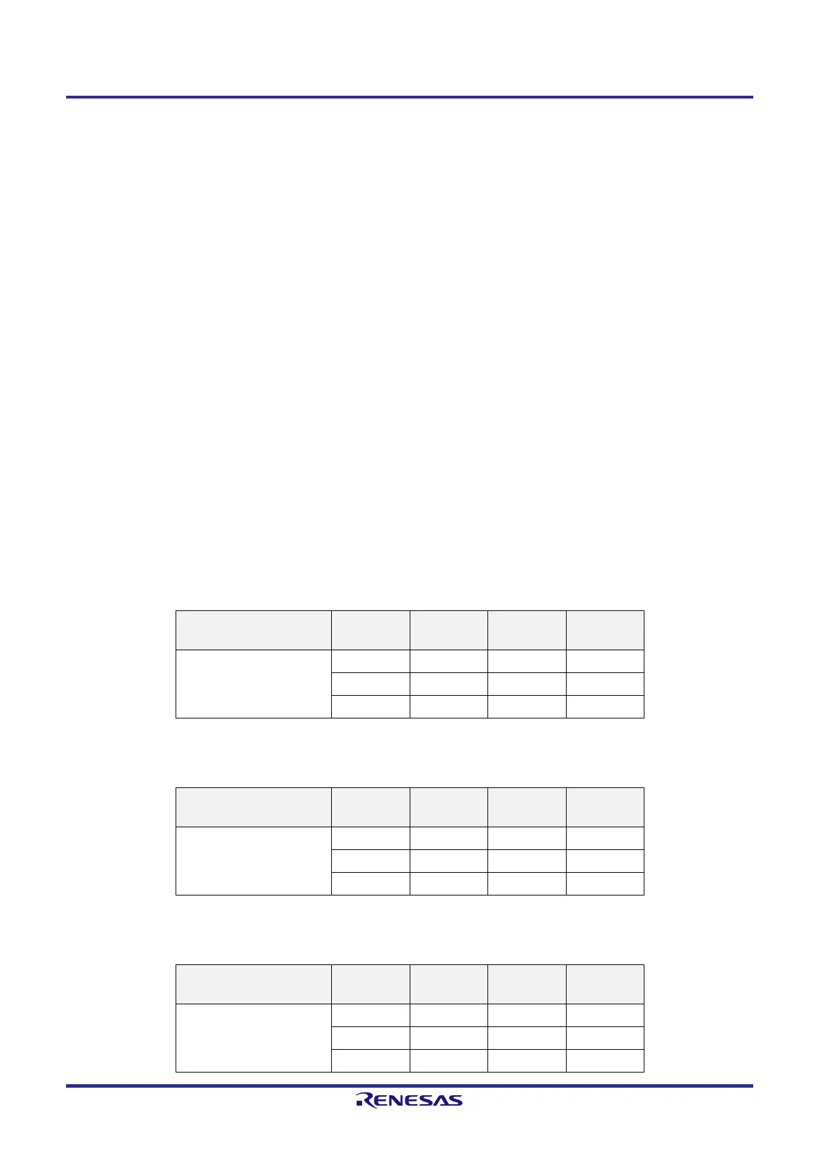
Examples 1: 99 + 89 = 188
Instruction A Register CY Flag AC Flag
BCDADJ
Register
MOV A, #99H ; <1>
99H
ADD A, #89H ; <2>
22H 1 1 66H
ADD A, !BCDADJ ; <3>
88H 1 0
Examples 2: 85 + 15 = 100
Instruction A Register CY Flag AC Flag
BCDADJ
Register
MOV A, #85H ; <1>
85H
ADD A, #15H ; <2>
9AH 0 0 66H
ADD A, !BCDADJ ; <3>
00H 1 1
Examples 3: 80 + 80 = 160
Instruction A Register CY Flag AC Flag
BCDADJ
Register
MOV A, #80H ; <1>
80H
ADD A, #80H ; <2>
00H 1 0 60H
ADD A, !BCDADJ ; <3>
60H 1 0

Table of Contents

Question and Answer IconNeed help?

Do you have a question about the Renesas RL78/G15 and is the answer not in the manual?

Renesas RL78/G15 Specifications

General IconGeneral
ArchitectureRL78
Maximum Operating Frequency32 MHz
Data Flashup to 4 KB
Pin Count20 to 64 pins
Timer Channelsup to 8
Communication InterfacesUART, I2C, SPI
Operating Voltage1.6 V to 5.5 V
Operating Temperature Range-40°C to +85°C
ADC10-bit
Timers16-bit timers, watchdog timer
Package TypesQFN, TSSOP

Summary

RL78/G15 User's Manual: Hardware

1.1 Features

Details low power consumption technology, RL78 CPU core architecture, memory capacities, and peripherals.

1.2 List of Part Numbers

Provides a breakdown of part numbers, indicating memory size, package, fields of application, and ROM capacity.

1.3 Pin Configuration (Top View)

Illustrates pin assignments and multiplexed functions for different product package types.

1.4 Pin Identification

Lists and describes the function of each pin, including alternate functions and their assignments.

1.5 Block Diagram

Provides block diagrams illustrating the internal structure and connections for various pin types.

1.6 Outline of Functions

Summarizes the functions available at the time peripheral I/O redirection register (PIOR) is set to 00H.

CHAPTER 2 PIN FUNCTIONS

2.1 Port Function

Details port input/output, buffer, and pull-up resistor settings, valid for alternate functions.

2.2 Functions other than port pins

Lists functions provided by pins that are not solely for port operations.

2.3 Connection of Unused Pins

Provides recommended connections for unused pins to prevent issues.

2.4 Block Diagrams of Pins

Shows block diagrams illustrating the functionality and connections of various pin types.

CHAPTER 3 CPU ARCHITECTURE

3.1 Overview

Describes the Harvard architecture, 3-stage pipeline, and main features of the RL78-S2 CPU core.

3.2 Memory Space

Details the 1-MB address space accessible by RL78/G15 products, including memory maps.

3.3 Processor Registers

Lists and describes the processor registers, including control registers, general-purpose registers, and ES/CS registers.

3.4 Instruction Address Addressing

Explains various addressing modes for instruction execution, including relative, immediate, and indirect addressing.

3.5 Addressing for Processing Data Addresses

Details addressing methods for data, including implied, register, direct, and indexed addressing.

3.6 Illegal Memory Access Detection Function

Describes the function that detects illegal memory access and generates a reset.

CHAPTER 4 PORT FUNCTIONS

4.1 Port Functions

Explains the digital I/O ports and their alternate functions, referring to Chapter 2 for details.

4.2 Port Configuration

Details the hardware components of ports, including mode registers, port registers, and pull-up resistors.

4.3 Registers Controlling Port Function

Lists registers used to control port functions, including mode, pull-up, and redirection registers.

4.4 Port Function Operations

Describes operations for I/O ports, differentiating between input and output modes.

4.5 Register Settings When Using Alternate Function

Explains register settings for using alternate functions, including basic concepts and examples.

4.6 Cautions When Using Port Function

Provides important cautions regarding port functions, especially for 1-bit manipulation and pin settings.

CHAPTER 5 CLOCK GENERATOR

5.1 Functions of Clock Generator

Describes the clock generator's role in supplying clocks to the CPU and peripheral hardware.

5.2 Configuration of Clock Generator

Details the hardware components of the clock generator, including control registers and oscillators.

5.3 Registers Controlling Clock Generator

Lists registers used to control the clock generator's operations.

5.4 System Clock Oscillator

Explains the X1 oscillator and on-chip oscillators, including their characteristics and usage.

5.5 Clock Generator Operation

Describes how the clock generator produces clocks and controls CPU operating modes like standby.

5.6 Controlling Clock

Provides examples and procedures for setting clock frequencies and managing clock switchover.

5.7 Resonator and Oscillator Constants

Refers to product pages for resonator operation verification and oscillator constants.

CHAPTER 6 TIMER ARRAY UNIT

6.1 Functions of Timer Array Unit

Overviews the functions of the timer array unit, including independent and simultaneous channel operations.

6.2 Configuration of Timer Array Unit

Details the hardware configuration of the timer array unit, including registers and I/O pins.

6.3 Registers Controlling Timer Array Unit

Lists registers used to control the timer array unit's operation.

6.4 Basic Rules of Timer Array Unit

Explains fundamental rules for simultaneous channel operation and 8-bit timer operation.

6.5 Operation of Counter

Describes the operation of the counter in different modes, including count clock and start timing.

6.6 Channel Output (TOmn pin) Control

Details the circuit configuration, setting, and cautions for TOmn pin output.

6.7 Timer Input (TImn) Control

Explains the TImn input circuit configuration, noise filter, and cautions for channel input.

6.8 Independent Channel Operation Function of Timer Array Unit

Describes specific functions of independent channels like interval timer and event counter.

6.9 Simultaneous Channel Operation Function of Timer Array Unit

Explains functions utilizing multiple channels, such as one-shot pulse and PWM output.

6.10 Cautions When Using Timer Array Unit

Provides important cautions related to using the timer array unit, especially for timer output.

CHAPTER 7 12-BIT INTERVAL TIMER

7.1 Functions of 12-bit Interval Timer

Describes the function of the 12-bit interval timer to generate interrupt requests at specified intervals.

7.2 Configuration of 12-bit Interval Timer

Details the hardware components of the 12-bit interval timer.

7.3 Registers Controlling 12-bit Interval Timer

Lists the registers used to control the 12-bit interval timer, including enable, speed mode, and control registers.

7.4 12-bit Interval Timer Operation

Explains the operation timing and procedures for starting count and entering HALT/STOP modes.

CHAPTER 8 CLOCK OUTPUT/BUZZER OUTPUT CONTROLLER

8.1 Functions of Clock Output/Buzzer Output Controller

Describes the functions of the clock output controller for peripheral ICs and buzzer output.

8.2 Configuration of Clock Output/Buzzer Output Controller

Details the hardware included in the clock output/buzzer output controller.

8.3 Registers Controlling Clock Output/Buzzer Output Controller

Lists registers used to control the clock output/buzzer output controller.

8.4 Operations of Clock Output/Buzzer Output Controller

Describes the operations of the clock output/buzzer output controller, including output pin behavior.

CHAPTER 9 WATCHDOG TIMER

9.1 Functions of Watchdog Timer

Explains the watchdog timer's function for detecting program loops and generating internal resets.

9.2 Configuration of Watchdog Timer

Details the hardware components of the watchdog timer, including control registers and option bytes.

9.3 Register Controlling Watchdog Timer

Lists the register used to control the watchdog timer.

9.4 Operation of Watchdog Timer

Describes how to control the watchdog timer's operation, including start, stop, and overflow time settings.

CHAPTER 10 A/D CONVERTER

10.1 Function of A/D Converter

Describes the A/D converter's function to convert analog signals to digital values.

10.2 Configuration of A/D Converter

Details the hardware components of the A/D converter, including input pins, sample & hold, and voltage comparator.

10.3 Registers Controlling A/D Converter

Lists registers used to control the A/D converter's operation and settings.

10.4 A/D Converter Conversion Operations

Describes the step-by-step process of A/D conversion operations.

10.5 Input Voltage and Conversion Results

Explains the relationship between analog input voltage and the resulting digital conversion value.

10.6 A/D Converter Operation Modes

Details the different operation modes of the A/D converter.

10.7 A/D Converter Setup Flowchart

Provides flowcharts for setting up the A/D converter for analog input and internal reference voltage.

10.8 How to Read A/D Converter Characteristics Table

Explains key terms and concepts for understanding A/D converter characteristics.

10.9 Notes on A/D Converter

Provides important notes and cautions regarding A/D converter usage, including conflicting operations and noise countermeasures.

CHAPTER 11 COMPARATOR

11.1 Comparator Functions

Lists the functions of the comparator, including selectable response speed and reference voltage.

11.2 Comparator Configuration

Describes the hardware components of the comparator, including input pins and output pins.

11.3 Registers Controlling the Comparator

Lists registers used to control the comparator's mode, filter, output, and port functions.

11.4 Comparator n Operation (n = 0, 1)

Details the operation of comparators 0 and 1, including digital filter and interrupt operations.

11.5 Comparator Setting Flowcharts

Provides flowcharts for enabling and disabling comparator operation.

CHAPTER 12 SERIAL ARRAY UNIT

12.1 Functions of Serial Array Unit

Overviews the functions of the serial array unit, including Simplified SPI, UART, and Simplified I2C.

12.2 Configuration of Serial Array Unit

Details the hardware components of the serial array unit, including registers and I/O pins.

12.3 Registers to Control the Serial Array Unit

Lists registers used to control the serial array unit's operation.

12.4 Operation Stop Mode

Describes the operation stop mode for serial interfaces to reduce power consumption.

12.5 Operation of Simplified SPI (CSI00, CSI01) Communication

Details the functions and operations of the Simplified SPI interface.

12.5.2 Master Reception

Describes the master reception operation where the microcontroller receives data via transfer clock.

12.5.3 Master Transmission/Reception

Explains master transmission/reception where data is transmitted/received via transfer clock.

12.5.4 Slave Transmission

Describes slave transmission where data is transmitted via transfer clock input from another device.

12.5.5 Slave Reception

Explains slave reception where data is received via transfer clock input from another device.

12.5.6 Slave Transmission/Reception

Details slave transmission/reception where data is transmitted/received via transfer clock input.

12.5.7 Calculating Transfer Clock Frequency

Provides formulas for calculating transfer clock frequency for simplified SPI communication.

12.5.8 Procedure for Processing Errors that Occurred During Simplified SPI (CSI00, CSI01) Communication

Describes procedures for processing errors like overrun error in SPI communication.

12.6 Operation of UART (UART0) Communication

Details the UART communication function, including data format, interrupts, and error detection.

12.7 Operation of Simplified I2C (IIC00, IIC01) Communication

Explains the simplified I2C communication, including address field, data transmission, and stop condition.

CHAPTER 13 SERIAL INTERFACE IICA

13.1 Functions of Serial Interface IICA

Overviews the three modes of the serial interface IICA: Operation stop, I2C bus, and Wakeup modes.

13.2 Configuration of Serial Interface IICA

Details the hardware components of the serial interface IICA, including registers and pins.

13.3 Registers Controlling Serial Interface IICA

Lists registers used to control the serial interface IICA, including enable, control, status, and flag registers.

13.4 I2C Bus Mode Functions

Describes the functions related to I2C bus mode, including pin configuration and transfer clock settings.

13.5 I2C Bus Definitions and Control Methods

Defines I2C bus terms and explains control methods like start/stop conditions, ACK, and clock stretching.

CHAPTER 14 INTERRUPT FUNCTIONS

14.1 Interrupt Function Types

Describes the two types of interrupt functions: maskable and software interrupts.

14.2 Interrupt Sources and Configuration

Lists interrupt sources and their configuration, including reset sources and vector codes.

14.3 Registers Controlling Interrupt Functions

Lists registers used to control interrupt functions, such as request flags, mask flags, and priority specifications.

14.4 Interrupt Servicing Operations

Explains the operations involved in servicing interrupts, including acknowledgment and multiple interrupt handling.

CHAPTER 15 STANDBY FUNCTION

15.1 Overview

Introduces the standby function for reducing system operating current, detailing HALT and STOP modes.

15.2 Registers controlling standby function

Lists registers that control the standby function, referring to Chapter 5 for clock generator details.

15.3 Standby Function Operation

Describes the operation of the HALT and STOP modes, including release conditions and operating status.

CHAPTER 16 RESET FUNCTION

16.1 Timing of Reset Operation

Details the timing of reset operation triggered by external or internal reset signals.

16.2 States of Operation During Reset Periods

Describes the states of operation and hardware after reset acceptance.

16.3 Register for Confirming Reset Source

Explains the RESF register used to store the source of the reset request.

CHAPTER 17 SELECTABLE POWER-ON-RESET CIRCUIT

17.1 Functions of Selectable Power-on-reset Circuit

Overviews the functions of the SPOR circuit, including internal reset generation and voltage detection.

17.2 Configuration of Selectable Power-on-reset Circuit

Shows the block diagram of the selectable power-on-reset circuit.

17.3 Operation of Selectable Power-on-reset Circuit

Describes the operation of the SPOR circuit, including internal reset signal generation timing.

17.4 Cautions for Selectable Power-on-reset Circuit

Provides cautions regarding the selectable power-on-reset circuit, especially concerning supply voltage fluctuations.

CHAPTER 18 OPTION BYTE

18.1 Functions of Option Bytes

Explains the option byte area, consisting of user option bytes and on-chip debug option bytes.

18.2 Format of User Option Byte

Details the format of the user option byte (000C0H), including watchdog timer and SPOR settings.

18.3 Format of On-chip Debug Option Byte

Shows the format of the on-chip debug option byte (000C3H) for controlling debug operations.

18.4 Setting of Option Byte

Describes how to specify the option byte using assembly language or link options.

CHAPTER 19 FLASH MEMORY

19.1 Serial Programming Using Flash Memory Programmer

Explains programming the flash memory using a dedicated programmer or external device via UART.

19.2 Writing to Flash Memory by Using External Device (that Incorporates UART)

Describes writing data to flash memory on-board via UART communication with an external device.

19.3 Connection of Pins on Board

Details the pin connections required for flash memory programming on the target system.

19.4 Serial Programming Method

Outlines the procedures for serial programming, including initial setup and stopping the process.

19.5 Processing Time for Each Command When PG-FP5 Is in Use (Reference Values)

Provides reference values for processing time for each command when using the PG-FP5 programmer.

19.6 Self-Programming

Describes the self-programming function for rewriting code/data flash memory via user program.

19.7 Data Flash

Provides an overview of the data flash memory, including its access methods and limitations.

CHAPTER 20 ON-CHIP DEBUG FUNCTION

20.1 Connecting E2, E2 Lite On-chip Debugging Emulator

Explains the connection example for the E2/E2 Lite emulator and RL78 microcontroller.

20.2 Connecting External Device (that Incorporates UART)

Describes the connection of an external device via UART for communication with the RL78 microcontroller.

20.3 On-Chip Debug Security ID

Details the on-chip debug security ID setting area for preventing third-party access to memory content.

20.4 Securing of User Resources

Explains the need for securing memory space before using debug functions.

CHAPTER 21 BCD CORRECTION CIRCUIT

21.1 BCD Correction Circuit Function

Describes the function of the BCD correction circuit for calculating BCD code results.

21.2 Registers Used by BCD Correction Circuit

Lists the registers used by the BCD correction circuit.

21.3 BCD Correction Circuit Operation

Explains the basic operation of the BCD correction circuit for addition and subtraction.

CHAPTER 22 INSTRUCTION SET

22.1 Conventions Used in Operation List

Explains conventions used for operand identifiers and specification methods in the operation list.

22.2 Operation List

Provides a comprehensive list of instructions, including mnemonic, operand, bytes, clock, operation, and flag details.

CHAPTER 23 ELECTRICAL SPECIFICATIONS (TA = −40 to +85°C)

23.1 Absolute Maximum Ratings

Lists the absolute maximum ratings for supply voltage, input/output voltage, and currents.

23.2 Oscillator Characteristics

Details the characteristics of the X1 oscillator and on-chip oscillators, including frequency and accuracy.

23.3 DC Characteristics

Provides DC electrical characteristics, including pin characteristics and supply current.

23.4 AC Characteristics

Lists AC timing parameters for various interfaces like SPI and UART.

23.5 Serial Interface Characteristics

Details the characteristics of serial interfaces, including UART, SPI, and I2C.

23.6 Analog Characteristics

Provides analog characteristics for A/D converters and comparators, including resolution and errors.

23.6.4 SPOR circuit characteristics

Details the characteristics of the SPOR circuit, including detection voltage and minimum pulse width.

23.6.5 Power supply voltage rising slope characteristics

Specifies the power supply voltage rising slope characteristics.

23.7 RAM Data Retention Characteristics

Describes RAM data retention characteristics related to power supply voltage.

23.8 Flash Memory Programming Characteristics

Details characteristics related to flash memory programming, including rewrite counts and programming times.

23.9 Dedicated Flash Memory Programmer Communication (UART)

Explains communication modes and transfer rates for dedicated flash memory programmers.

23.10 Timing of Entry to Flash Memory Programming Mode

Shows timing diagrams for entering flash memory programming mode.

CHAPTER 24 ELECTRICAL SPECIFICATIONS (TA = −40 to +105°C, TA = −40 to +125°C)

24.1 Absolute Maximum Ratings

Lists the absolute maximum ratings for supply voltage, input/output voltage, and currents.

24.2 Oscillator Characteristics

Details the characteristics of the X1 oscillator and on-chip oscillators, including frequency and accuracy.

24.3 DC Characteristics

Provides DC electrical characteristics, including pin characteristics and supply current.

24.4 AC Characteristics

Lists AC timing parameters for various interfaces like SPI and UART.

24.5 Serial Interface Characteristics

Details the characteristics of serial interfaces, including UART, SPI, and I2C.

24.6 Analog Characteristics

Provides analog characteristics for A/D converters and comparators, including resolution and errors.

24.6.4 SPOR circuit characteristics

Details the characteristics of the SPOR circuit, including detection voltage and minimum pulse width.

24.6.5 Power supply voltage rising slope characteristics

Specifies the power supply voltage rising slope characteristics.

24.7 RAM Data Retention Characteristics

Describes RAM data retention characteristics related to power supply voltage.

24.8 Flash Memory Programming Characteristics

Details characteristics related to flash memory programming, including rewrite counts and programming times.

24.9 Dedicated Flash Memory Programmer Communication (UART)

Explains communication modes and transfer rates for dedicated flash memory programmers.

24.10 Timing of Entry to Flash Memory Programming Mode

Shows timing diagrams for entering flash memory programming mode.

CHAPTER 25 PACKAGE DRAWINGS

25.1 8-pin products

Provides package drawing details for 8-pin products.

25.2 10-pin products

Provides package drawing details for 10-pin products.

25.3 16-pin products

Provides package drawing details for 16-pin products.

25.4 20-pin products

Provides package drawing details for 20-pin products.

APPENDIX A REVISION HISTORY

A.1 Major Revisions in This Edition

Lists major revisions made in the current edition of the manual.

A.2 Revision History of Preceding Editions

Provides a revision history of preceding editions of the manual.

Related product manuals