RL78/G15 CHAPTER 10 A/D CONVERTER
R01UH0959EJ0110 Rev.1.10 Page 343 of 765
Mar 7, 2023
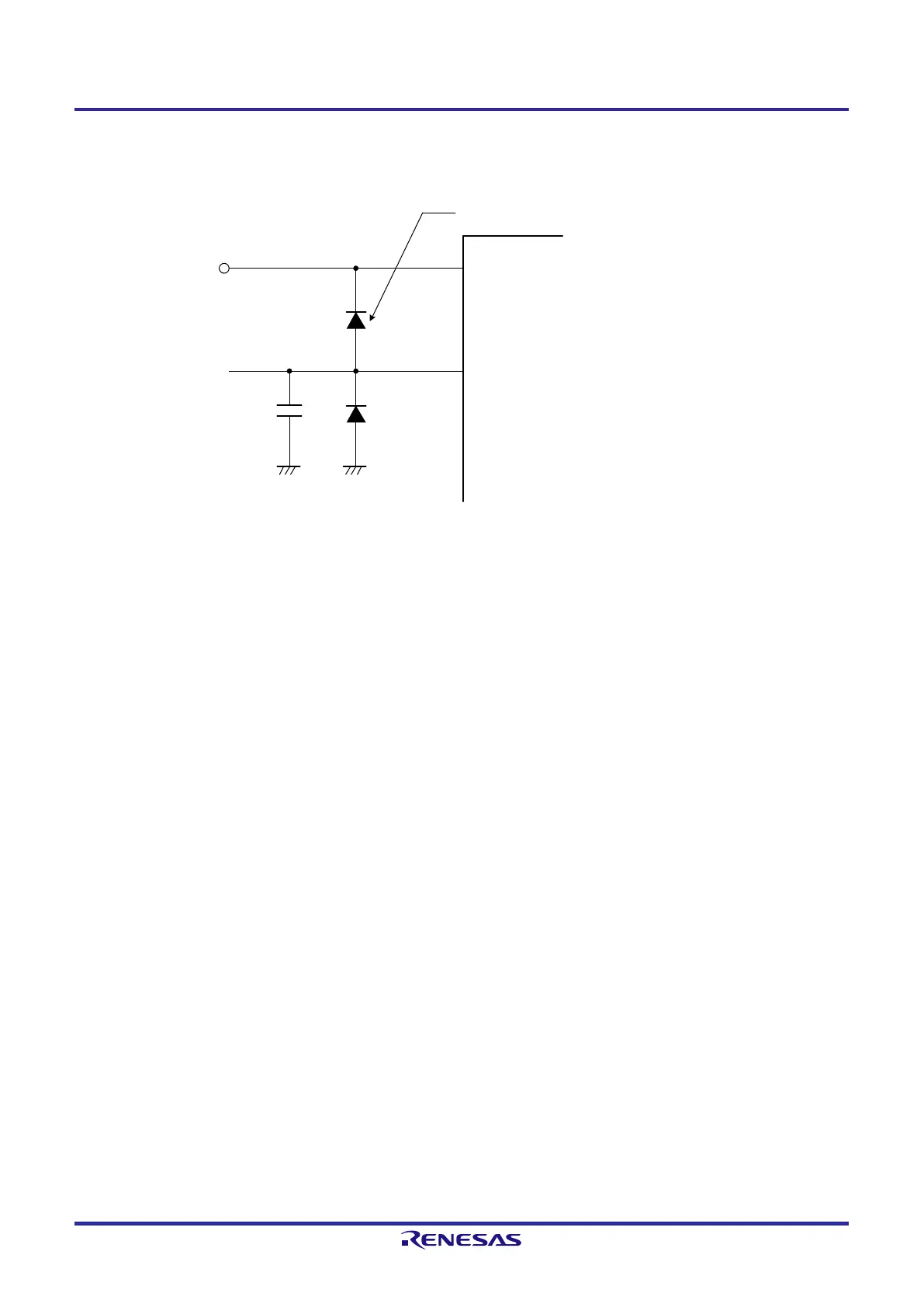
Figure 10-22. Analog Input Pin Connection
ANI0 to ANI10
Reference
voltage input
C = 10 pF to 0.1 μF
If there is a possibility that noise equal to or higher than V
DD
or
equal to or lower than V
SS
may enter
, clamp with a diode with a
small V
F
value (0.3 V or lower).
V
DD
10.9.5 Analog input (ANIn) pins
(1) The analog input pins (ANI0 to ANI10
Note 1
) are also used as input port pins (P01 to P07
Note 2
and P20 to P23
Note 2
).
When A/D conversion is performed with any of the ANI0 to ANI10 pins selected, do not change output values to
alternate port P01 to P07
Note 2
and P20 to P23
Note 2
while conversion is in progress; otherwise the conversion
accuracy may be degraded.
(2) If a pin adjacent to a pin that is being A/D converted is used as a digital I/O port pin, the A/D conversion result
might differ from the expected value due to a coupling noise. Be sure to prevent such a pulse from being input or
output.
Note 1. ANI0, ANI2, ANI3 for 8-pin products,
ANI0 to ANI3 for 10-pin products,
ANI0 to ANI6 for 16-pin products
Note 2. P01, P03, P04 for 8-pin products,
P01 to P04 for 10-pin products,
P01 to P07 for 16-pin products
 Loading...


