RL78/G15 CHAPTER 5 CLOCK GENERATOR
R01UH0959EJ0110 Rev.1.10 Page 155 of 765
Mar 7, 2023
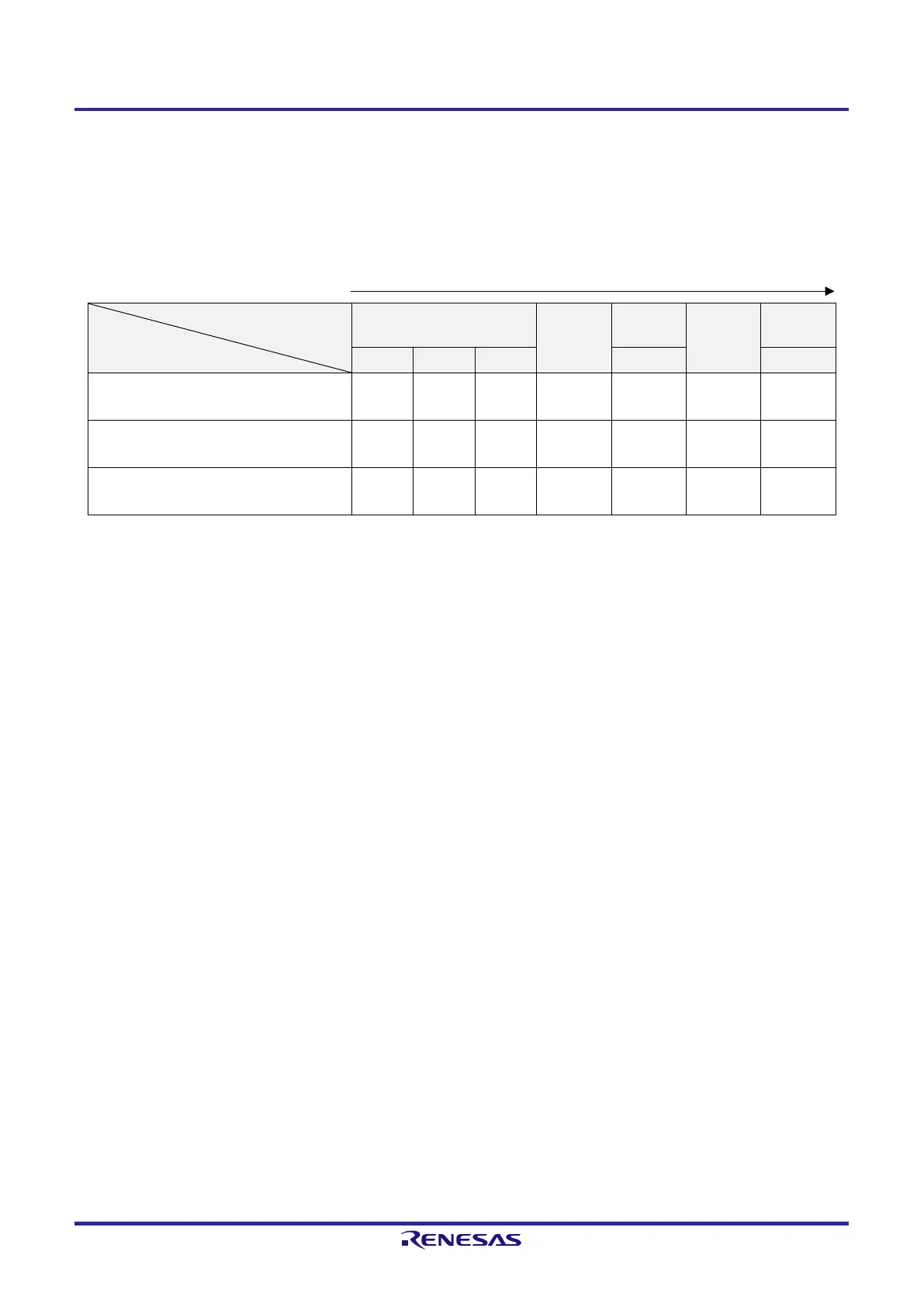
Table 5-3 shows transition of the CPU clock and examples of setting the SFR registers.
Table 5-3. CPU Clock Transition and SFR Register Setting Examples for 16-Pin and 20-Pin Products (1/2)
(1) CPU clock changing from high-speed on-chip oscillator clock (A) to high-speed system clock (B) (The CPU
operates with the high-speed on-chip oscillator clock immediately after a reset release (A).)
(Setting sequence of SFR registers)
Setting Flag of SFR Register
Status Transition
CMC Register
Note 1
OSTS
Register
CSC
Register
OSTC
Register
CKC
Register
EXCLK OSCSEL AMPH MSTOP MCM0
(A) → (B)
(X1 clock: 1 MHz ≤ f
X
≤ 10 MHz)
0 1 0
Note 2
0
Must be
checked
1
(A) → (B)
(X1 clock: 10 MHz < f
X
≤ 12 MHz)
0 1 1
Note 2
0
Must be
checked
1
(A) → (B)
(External main system clock)
1 1 ×
Note 2
0
Must be
checked
1
Note 1. The clock operation mode control register (CMC) can be written only once by an 8-bit memory manipulation
instruction after reset release.
Note 2. Set the oscillation stabilization time as follows.
Desired the oscillation stabilization time counter status register (OSTC) oscillation stabilization time ≤
Oscillation stabilization time set by the oscillation stabilization time select register (OSTS)
Caution Set the clock after the supply voltage has reached the operable voltage of the clock to be set (see
CHAPTER 23 ELECTRICAL SPECIFICATIONS (T
A
= −40 to +85°C) and CHAPTER 24 ELECTRICAL
SPECIFICATIONS) (T
A
= −40 to +105°C, T
A
= −40 to +125°C).
Remark 1. ×: Don’t care
Remark 2. (A) to (F) in Table 5-3 correspond to (A) to (F) in Figure 5-14.
 Loading...


