R01UH0823EJ0100 Rev.1.00 Page 1437 of 1823
Jul 31, 2019
RX23W Group 40. SD Host Interface (SDHIa)
40.2.12 Card Access Option Register (SDOPT)
Note 1. Do not rewrite these bits when the SDSTS2.CBSY flag is 1.
The SD bus width and timeout counter are set in the SDOPT register.
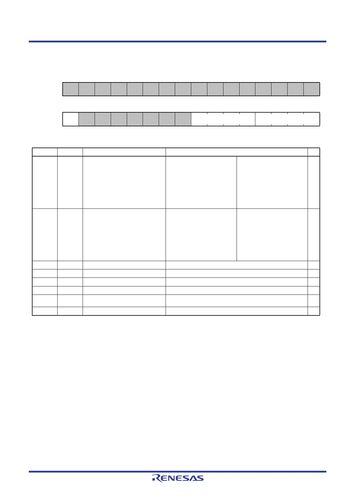
SDOPT
Address SDHI.SDOPT 0008 AC50h
b31 b30 b29 b28 b27 b26 b25 b24 b23 b22 b21 b20 b19 b18 b17 b16
— — — — — — — — — — — — — — — —
Value after reset
0000000000000000
b15 b14 b13 b12 b11 b10 b9 b8 b7 b6 b5 b4 b3 b2 b1 b0
WIDTH
— — — — — — —
TOP[3:0] CTOP[3:0]
Value after reset
0100000011101110
Bit Symbol Bit Name Description R/W
b3 to b0 CTOP[3:0] Card Detection Time Counter
*1
b3 b0
0 0 0 0: PCLKB × 2
10
0 0 0 1: PCLKB × 2
11
0 0 1 0: PCLKB × 2
12
0 0 1 1: PCLKB × 2
13
0 1 0 0: PCLKB × 2
14
0 1 0 1: PCLKB × 2
15
0 1 1 0: PCLKB × 2
16
0 1 1 1: PCLKB × 2
17
b3 b0
1 0 0 0: PCLKB × 2
18
1 0 0 1: PCLKB × 2
19
1 0 1 0: PCLKB × 2
20
1 0 1 1: PCLKB × 2
21
1 1 0 0: PCLKB × 2
22
1 1 0 1: PCLKB × 2
23
1 1 1 0: PCLKB × 2
24
1 1 1 1: Do not set this value.
R/W
b7 to b4 TOP[3:0] Timeout Counter
*1
b7 b4
0 0 0 0: SDHI clock × 2
13
0 0 0 1: SDHI clock × 2
14
0 0 1 0: SDHI clock × 2
15
0 0 1 1: SDHI clock × 2
16
0 1 0 0: SDHI clock × 2
17
0 1 0 1: SDHI clock × 2
18
0 1 1 0: SDHI clock × 2
19
0 1 1 1: SDHI clock × 2
20
b7 b4
1 0 0 0: SDHI clock × 2
21
1 0 0 1: SDHI clock × 2
22
1 0 1 0: SDHI clock × 2
23
1 0 1 1: SDHI clock × 2
24
1 1 0 0: SDHI clock × 2
25
1 1 0 1: SDHI clock × 2
26
1 1 1 0: SDHI clock × 2
27
1 1 1 1: Do not set this value.
R/W
b8 — Reserved This bit is 0 when read. Set it to 0 when writing. R/W
b12 to b9 — Reserved These bits are 0 when read and cannot be modified. R
b13 — Reserved This bit is 0 when read. Set it to 0 when writing. R/W
b14 — Reserved This bit is 1 when read and cannot be modified. R
b15 WIDTH SD Bus Width Select
*1
0: Wide bus mode (4 bits)
1: Default bus mode (1 bit)
R/W
b31 to b16 — Reserved These bits are 0 when read and cannot be modified. R

 Loading...


