R01UH0823EJ0100 Rev.1.00 Page 1744 of 1823
Jul 31, 2019
RX23W Group 51. Electrical Characteristics
51. Electrical Characteristics
51.1 Absolute Maximum Ratings
Caution: Permanent damage to the MCU may be caused if absolute maximum ratings are exceeded.
To preclude any malfunctions due to noise interference, insert capacitors with high frequency characteristics between the VCC
and VSS pins, between the AVCC0 and AVSS0 pins, between the VCC_USB and VSS_USB pins, between the VREFH0 and
VREFL0 pins, between the VCC_RF and VSS_RF pins, and between the AVCC_RF and VSS_RF pins. Place capacitors with
values of about 2.2 μF in the case of the VCC_RF pin and about 0.1 μF otherwise as close as possible to every power supply pin,
and use the shortest and thickest possible traces for the connections.
Connect the VCL pin to a VSS pin via a 4.7 μF capacitor. The capacitor must be placed close to the pin. For details, refer to
section 51.16.1, Connecting VCL Capacitor and Bypass Capacitors.
Do not input signals or an I/O pull-up power supply to ports other than 5-V tolerant ports while the device is not powered.
The current injection that results from input of such a signal or I/O pull-up may cause malfunction and the abnormal current that
passes in the device at this time may cause degradation of internal elements. Even if –0.3 to +6.5 V is input to 5-V tolerant ports,
it will not cause problems such as damage to the MCU.
Note 1. Ports 16, 17, 30, 31, and B5 are 5 V tolerant.
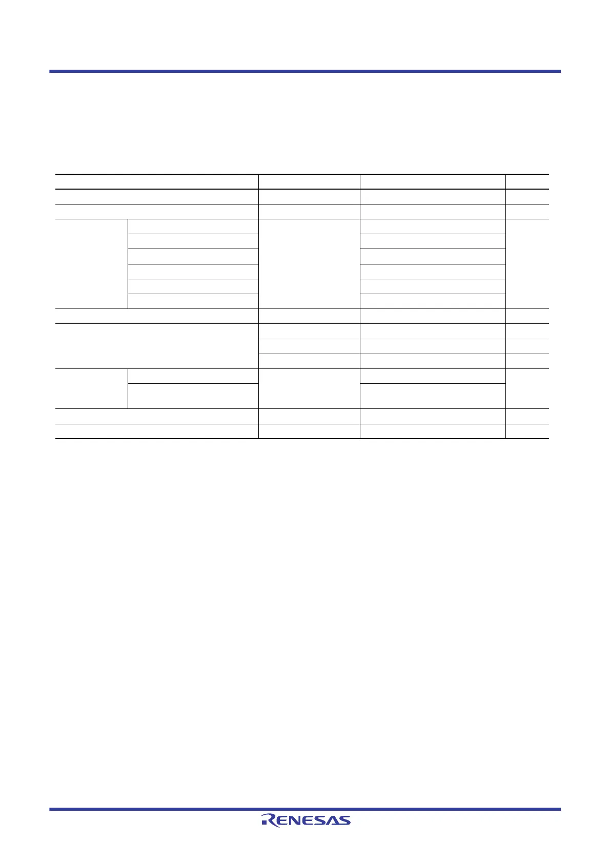
Table 51.1 Absolute Maximum Ratings
Conditions: VSS = AVSS0 = VREFL0 = VREFL = VSS_USB = VSS_RF = 0 V
Item Symbol Value Unit
Power supply voltage VCC, VCC_USB –0.3 to +4.0 V
VBATT power supply voltage VBATT –0.3 to +4.0 V
Input voltage Ports for 5 V tolerant*
1
V
in
–0.3 to +6.5 V
P03, P05, P07, P40 to P47 –0.3 to AVCC0 + 0.3
ANT –1.0 to +1.4
XTAL1_RF, XTAL2_RF –0.3 to +1.4
DCLIN_A, DCLIN_D –0.3 to +2.2
Ports other than above –0.3 to VCC + 0.3
Reference power supply voltage VREFH0 –0.3 to AVCC0 + 0.3 V
Analog power supply voltage AVCC0 –0.3 to +4.0 V
VCC_RF –0.3 to +4.0 V
AVCC_RF –0.3 to +4.0 V
Analog input
voltage
When AN000 to AN007 are used V
AN
–0.3 to AVCC0 + 0.3 V
When AN016 to AN020, AN027
are used
–0.3 to VCC + 0.3
Operating temperature T
opr
–40 to +85 °C
Storage temperature T
stg
–55 to +125 °C

 Loading...


