R01UH0823EJ0100 Rev.1.00 Page 517 of 1823
Jul 31, 2019
RX23W Group 23. Multi-Function Timer Pulse Unit 2 (MTU2a)
23.2.30 Noise Filter Control Registers (NFCR)
Note 1. These bits are reserved in MTU1 and MTU2. These bits are read as 0, and writing to them is not possible.
Note 2. These bits are reserved in MTU0, MTU1 and MTU2. These bits are read as 0, and writing to them is not possible.
The MTUn.NFCR registers (n = 0 to 4) enable and disable the noise filters for the MTIOCnm (n = 0 to 4; m = A to D)
pins and sets the sampling clocks for the noise filters.
NFAEN Bit (Noise Filter A Enable)
This bit disables or enables the noise filter for input from the MTIOCnA pin. Since unexpected edges may be internally
generated when the value of the NFAEN bit is changed, select the output compare function in the timer I/O control
register and set the TMDR.MD[3:0] bits to a value other than 0000b (normal mode) before changing the value.
NFBEN Bit (Noise Filter B Enable)
This bit disables or enables the noise filter for input from the MTIOCnB pin. Since unexpected edges may be internally
generated when the value of the NFBEN bit is changed, select the output compare function in the timer I/O control
register and set the TMDR.MD[3:0] bits to a value other than 0000b (normal mode) before changing the value.
NFCEN Bit (Noise Filter C Enable)
This bit disables or enables the noise filter for input from the MTIOCnC pin. Since unexpected edges may be internally
generated when the value of the NFCEN bit is changed, select the output compare function in the timer I/O control
register and set the TMDR.MD[3:0] bits to a value other than 0000b (normal mode) before changing the value.
NFDEN Bit (Noise Filter D Enable)
This bit disables or enables the noise filter for input from the MTIOCnD pin. Since unexpected edges may be internally
generated when the value of the NFDEN bit is changed, select the output compare function in the timer I/O control
register and set the TMDR.MD[3:0] bits to a value other than 0000b (normal mode) before changing the value.
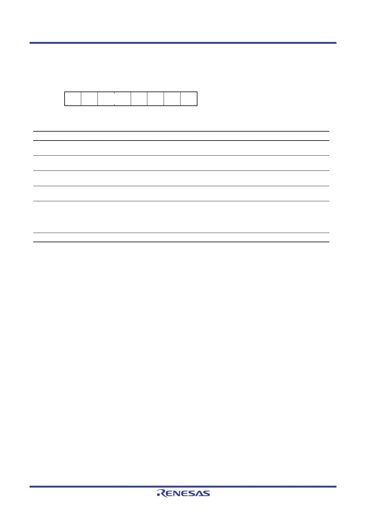
Address(es): MTU0.NFCR 000D 0A90h, MTU1.NFCR 000D 0A91h, MTU2.NFCR 000D 0A92h, MTU3.NFCR 000D 0A93h,
MTU4.NFCR 000D 0A94h
b7 b6 b5 b4 b3 b2 b1 b0
— — NFCS[1:0] NFDEN NFCEN NFBEN NFAEN
Value after reset:
00000000
Bit Symbol Bit Name Description R/W
b0 NFAEN Noise Filter A Enable 0: The noise filter for the MTIOCnA pin is disabled
1: The noise filter for the MTIOCnA pin is enabled
R/W
b1 NFBEN Noise Filter B Enable 0: The noise filter for the MTIOCnB pin is disabled
1: The noise filter for the MTIOCnB pin is enabled
R/W
b2 NFCEN Noise Filter C Enable*
1
0: The noise filter for the MTIOCnC pin is disabled
1: The noise filter for the MTIOCnC pin is enabled
R/W
b3 NFDEN Noise Filter D Enable*
2
0: The noise filter for the MTIOCnD pin is disabled
1: The noise filter for the MTIOCnD pin is enabled
R/W
b5, b4 NFCS[1:0] Noise Filter Clock Select
b5 b4
0 0: PCLK/1
0 1: PCLK/8
1 0: PCLK/32
1 1: The clock source for counting is the external clock
R/W
b7, b6 — Reserved These bits are read as 0. The write value should be 0. R/W
 Loading...


