R01UH0823EJ0100 Rev.1.00 Page 783 of 1823
Jul 31, 2019
RX23W Group 28. Realtime Clock (RTCe)
28.2.19 RTC Control Register 3 (RCR3)
The RCR3 register is used for controlling the sub-clock oscillator in the clock generation circuit. For details on
controlling the sub-clock oscillator, refer to
section 9, Clock Generation Circuit.
This register is a function common to calendar count mode and binary count mode.
When this register is modified, check that all the bits have been updated before proceeding to the next processing.
RTCEN Bit (Sub-Clock Oscillator Control)
The RTCEN bit and a clock generation circuit register (the SOSCCR.SOSTP bit) control whether to operate or stop the
sub-clock oscillator. If one of the bits is set so as to enable the operation, the sub-clock oscillator runs.
When using the sub-clock as the count source to the RTC, set the sub-clock oscillator using the RTCEN bit.
RTCDV[2:0] Bits (Sub-Clock Oscillator Drive Capacity Control)
These bits control the drive capacity of the sub-clock oscillator. Set the RTCDV[2:0] bits when the SOSCCR.SOSTP bit
is 1 and the RCR3.RTCEN bit is 0.
28.2.19.1 Notes on using a low CL crystal unit
When the signal level of any pin near the XCIN or XCOUT pin is changed, the oscillation accuracy of the sub-clock
oscillator may be affected. The accuracy is affected differently depending on the board traces and how the signal level of
any pin near the XCIN or XCOUT pin is changed. When designing a board using a low CL crystal unit, refer to the
application note “Design Guide for Low CL Sub-clock Circuits” (R01AN1012EJ) to reduce the influence from noise.
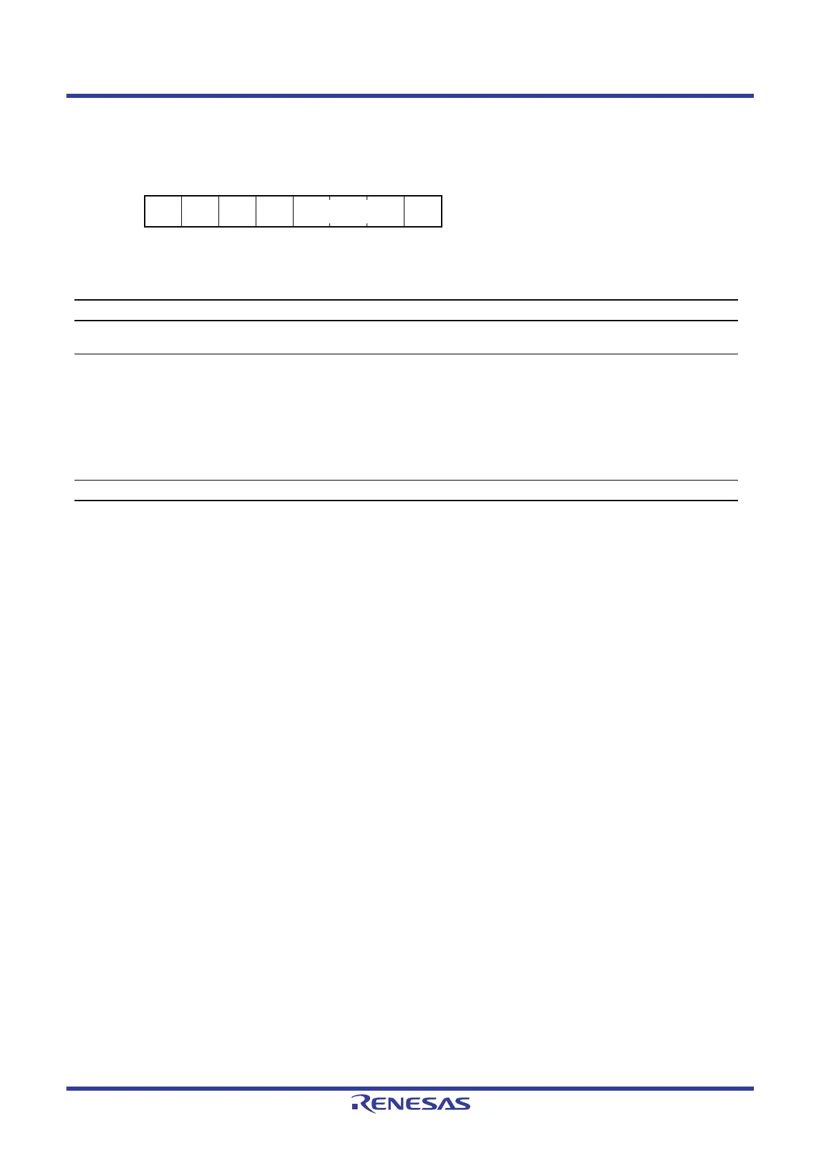
Address(es): RTC.RCR3 0008 C426h
b7 b6 b5 b4 b3 b2 b1 b0
———— RTCDV[2:0] RTCEN
Value after reset:
0000xxxx
x: Undefined
Bit Symbol Bit Name Description R/W
b0 RTCEN Sub-Clock Oscillator Control 0: Sub-clock oscillator is stopped.
1: Sub-clock oscillator is operating.
R/W
b3 to b1 RTCDV[2:0] Sub-Clock Oscillator Drive
Capacity Control
b3 b1
0 0 0: Setting prohibited
0 0 1: Drive capacity for low CL
0 1 0: Setting prohibited
0 1 1: Setting prohibited
1 0 0: Setting prohibited
1 0 1: Setting prohibited
1 1 0: Drive capacity for standard CL
1 1 1: Setting prohibited
R/W
b7 to b4 — Reserved These bits are read as 0. The write value should be 0. R/W