R01UH0823EJ0100 Rev.1.00 Page 508 of 1823
Jul 31, 2019
RX23W Group 23. Multi-Function Timer Pulse Unit 2 (MTU2a)
23.2.19 Timer Output Level Buffer Registers (TOLBR)
The TOLBR registers function as buffer registers for the TOCR2 register and specify the PWM output level in
complementary PWM mode and reset-synchronized PWM mode.
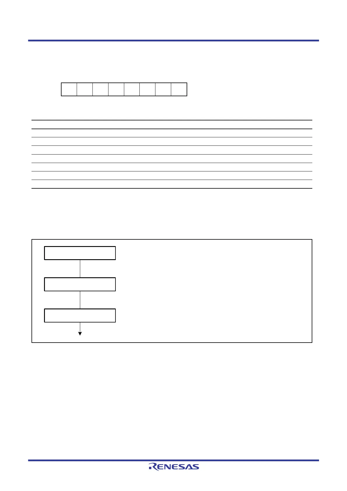
Figure 23.3 shows an example of the PWM output level setting procedure in buffer operation.
Figure 23.3 Example of PWM Output Level Setting Procedure in Buffer Operation
Address(es): MTU.TOLBR 000D 0A36h
b7 b6 b5 b4 b3 b2 b1 b0
— — OLS3N OLS3P OLS2N OLS2P OLS1N OLS1P
Value after reset:
00000000
Bit Symbol Bit Name Description R/W
b0 OLS1P Output Level Select 1P Specify the buffer value to be transferred to the OLS1P bit in TOCR2. R/W
b1 OLS1N Output Level Select 1N Specify the buffer value to be transferred to the OLS1N bit in TOCR2. R/W
b2 OLS2P Output Level Select 2P Specify the buffer value to be transferred to the OLS2P bit in TOCR2. R/W
b3 OLS2N Output Level Select 2N Specify the buffer value to be transferred to the OLS2N bit in TOCR2. R/W
b4 OLS3P Output Level Select 3P Specify the buffer value to be transferred to the OLS3P bit in TOCR2. R/W
b5 OLS3N Output Level Select 3N Specify the buffer value to be transferred to the OLS3N bit in TOCR2. R/W
b7, b6 — Reserved These bits are read as 0. The write value should be 0. R/W
[1] Set the TOCR1.TOCS bit to 1 to enable the TOCR2 register setting.
[2] Use the TOCR2.BF[1:0] bits to select the TOLBR buffer transfer timing.
Use bits OLS3N to OLS1N and OLS3P to OLS1P to specify the PWM
output levels.
[3] The TOLBR register initial setting must be the same value as specified
in bits OLS3N to OLS1N and OLS3P to OLS1P in the TOCR2 register.
Set the TOCS bit
Set the TOCR2 register
Set the TOLBR register
[1]
[2]
[3]

 Loading...


