R01UH0823EJ0100 Rev.1.00 Page 1643 of 1823
Jul 31, 2019
RX23W Group 47. Comparator B (CMPBa)
47.2.8 Comparator B1 Output Control Register (CPB1OCR)
Note 1. When the CPBnOE bit (n = 2, 3) is set to 0 to disable the CMPOBn pin output, 0 is output to CMPOBn regardless of the value of
the CPBnOP bit.
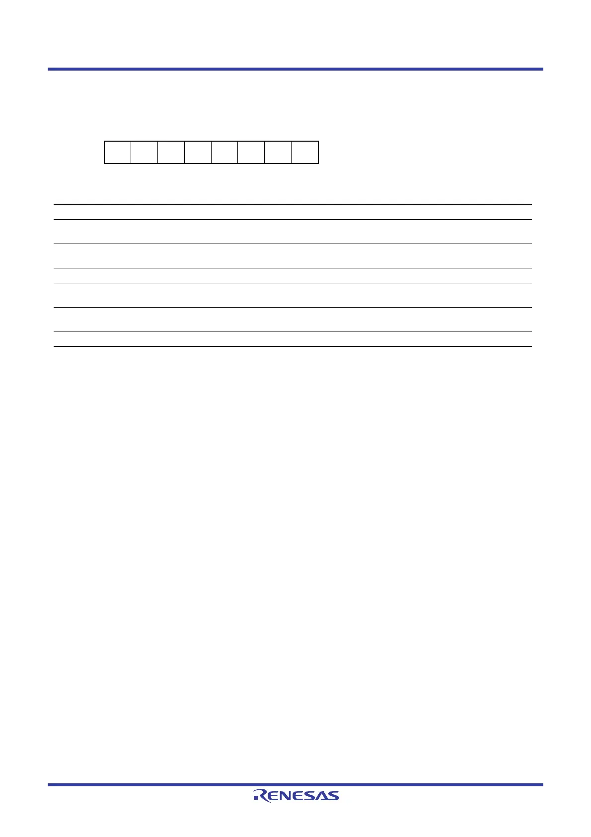
Address: 0008 C5A7h
b7 b6 b5 b4 b3 b2 b1 b0
——
CPB3O
P
CPB3O
E
——
CPB2O
P
CPB2O
E
Value after reset:
00000000
Bit Symbol Bit Name Description R/W
b0 CPB2OE CMPOB2 Pin Output Enable 0: Comparator B2 CMPOB2 pin output disabled*
1
1: Comparator B2 CMPOB2 pin output enabled
R/W
b1 CPB2OP CMPOB2 Output Polarity Select 0: Comparator B2 output is output to CMPOB2
1: Inverted comparator B2 output is output to CMPOB2
RW
b3, b2 — Reserved These bits are read as 0. The write value should be 0. RW
b4 CPB3OE CMPOB3 Pin Output Enable 0: Comparator B3 CMPOB3 pin output disabled*
1
1: Comparator B3 CMPOB3 pin output enabled
RW
b5 CPB3OP CMPOB3 Output Polarity Select 0: Comparator B3 output is output to CMPOB3
1: Inverted comparator B3 output is output to CMPOB3
RW
b7, b6 — Reserved These bits are read as 0. The write value should be 0. RW

 Loading...


