R01UH0823EJ0100 Rev.1.00 Page 385 of 1823
Jul 31, 2019
RX23W Group 19. Data Transfer Controller (DTCa)
19.2.6 DTC Transfer Count Register B (CRB)
CRB register is used to set the block transfer count for block transfer mode and cannot be accessed directly from the
CPU.
The transfer count is 1, 65535, and 65536 when the set value is 0001h, FFFFh, and 0000h, respectively.
The CRB value is decremented (–1) when the final data of a single block size is transferred.
When normal transfer mode or repeat transfer mode is selected, this register is not used and the set value is ignored.
19.2.7 DTC Control Register (DTCCR)
DTCCR register is used to control the DTC operation.
RRS Bit (DTC Transfer Information Read Skip Enable)
The DTC vector number is compared with the vector number in the previous data transfer.
When these vector numbers match and the RRS bit is set to 1, DTC data transfer is performed without reading the
transferred information. However, when the previous transfer was chain transfer, the transferred information is read
regardless of the value of the RRS bit.
Furthermore, when the transfer counter (CRA register) became 0 during the previous normal transfer and when the
transfer counter (CRB register) became 0 during the previous block transfer, the transferred information is read
regardless of the RRS bit value.
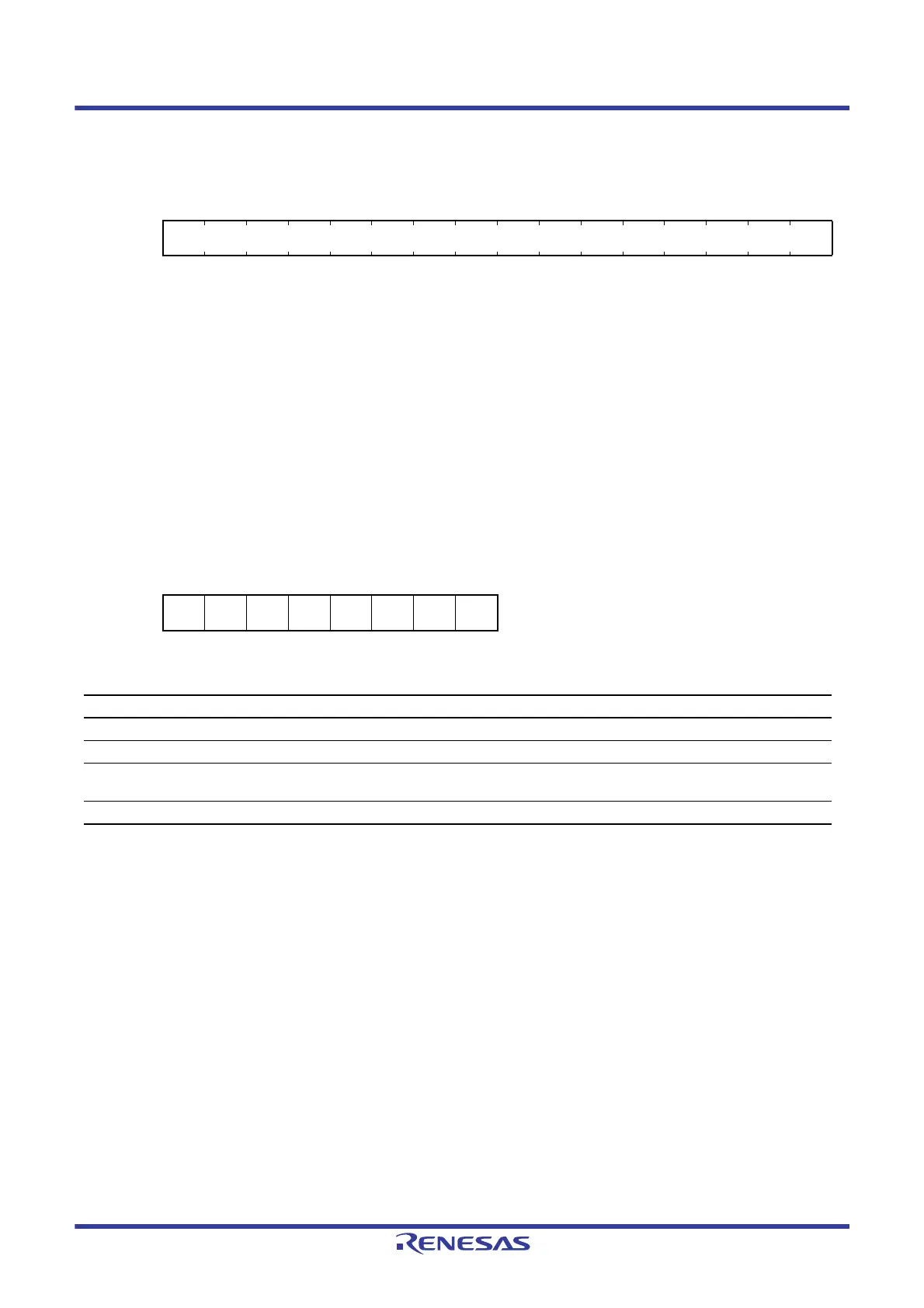
Address(es): (inaccessible directly from the CPU)
b15 b14 b13 b12 b11 b10 b9 b8 b7 b6 b5 b4 b3 b2 b1 b0
Value after reset:
xxxxxxxxxxxxxxxx
x: Undefined
Address(es): DTC.DTCCR 0008 2400h
b7 b6 b5 b4 b3 b2 b1 b0
———RRS————
Value after reset:
00001000
Bit Symbol Bit Name Description R/W
b2 to b0 — Reserved These bits are read as 0. The write value should be 0. R/W
b3 — Reserved This bit is read as 1. The write value should be 1. R/W
b4 RRS DTC Transfer Information
Read Skip Enable
0: Transfer information read is not skipped.
1: Transfer information read is skipped when vector numbers match.
R/W
b7 to b5 — Reserved These bits are read as 0. The write value should be 0. R/W

 Loading...


