EasyManuals Logo

Renesas RX Series User Manual

Renesas RX Series
1823 pages
To Next Page IconTo Next Page
To Previous Page IconTo Previous Page
Page #1043 background image
R01UH0823EJ0100 Rev.1.00 Page 1043 of 1823
Jul 31, 2019
RX23W Group 33. Serial Communications Interface (SCIg, SCIh)
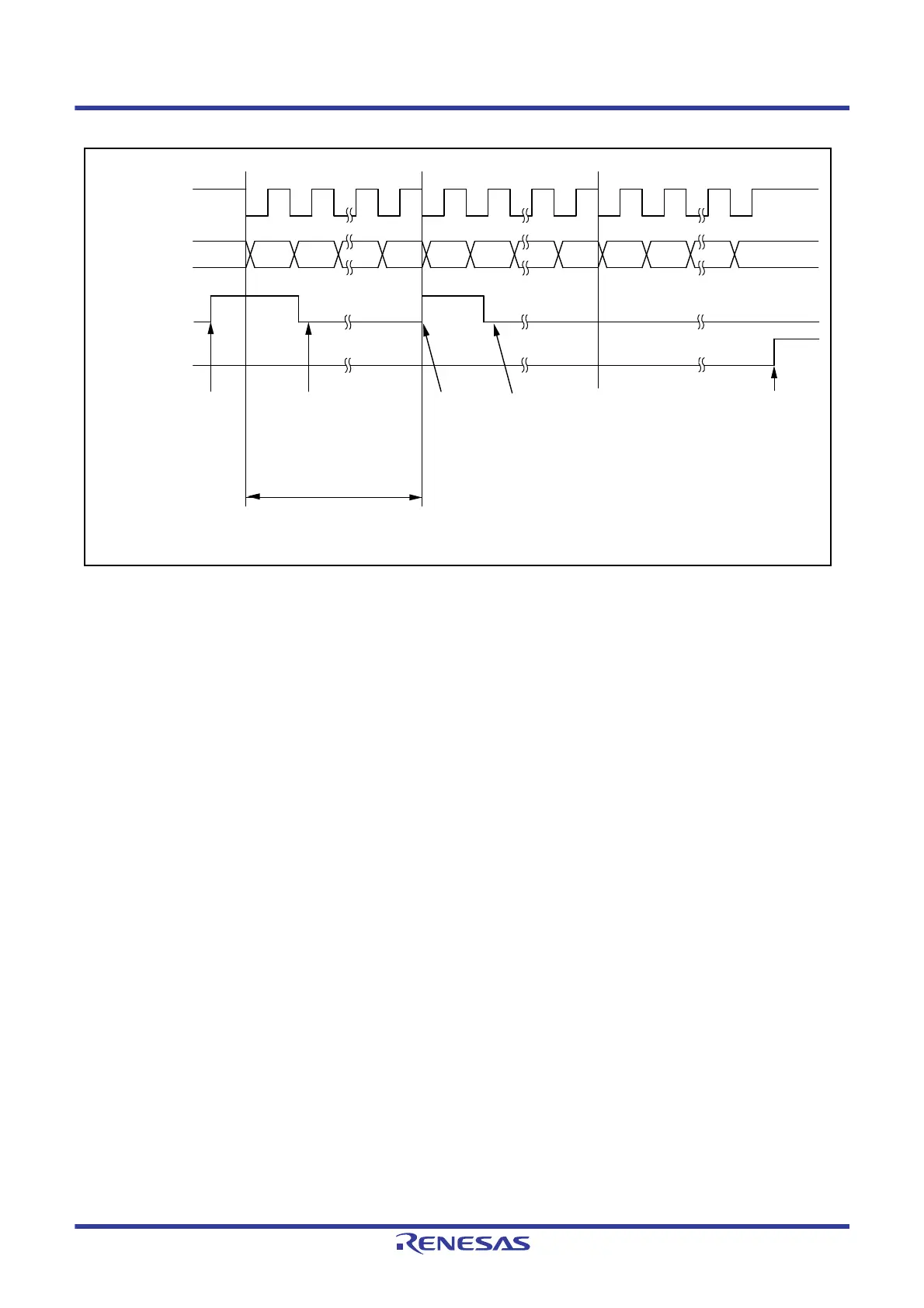
Figure 33.27 Example of Serial Data Transmission in Clock Synchronous Mode from the Middle of
Transmission until Transmission Completion
Synchronization
clock
1 frame
Serial data
TXI interrupt
request
generated
TEI interrupt
request
generated
TXI interrupt
request
generated
TXI interrupt flag
(IRn in ICU*
1
)
Data written to TDR in
TXI interrupt handling
routine
SSR.TEND flag
(TIE = 1)
(TIE = 0)
Bit 0 Bit 1 Bit 7 Bit 0 Bit 1 Bit 7 Bit 0
Bit 1 Bit 7
Data written to TDR in TXI
interrupt handling routine
(Set the TIE bit to 0 and the
TEIE bit to 1 after writing the
last data)
Note 1. Refer to section 15, Interrupt Controller (ICUb) for details on the corresponding interrupt vector number.

Table of Contents

Questions and Answers:

Question and Answer IconNeed help?

Do you have a question about the Renesas RX Series and is the answer not in the manual?

Renesas RX Series Specifications

General IconGeneral
CoreRXv1, RXv2, RXv3
Flash MemoryUp to 8 MB
RAMUp to 1 MB
Operating Voltage1.62V to 5.5V
Operating Temperature-40°C to +85°C or +105°C
PackageBGA, LQFP
ADC Resolution12-bit
DAC Resolution12-bit
Communication InterfacesSCI, SPI, I2C, USB, Ethernet, CAN
Architecture32-bit
Security FeaturesMemory Protection Unit (MPU)

Related product manuals