R01UH0823EJ0100 Rev.1.00 Page 1608 of 1823
Jul 31, 2019
RX23W Group 44. 12-Bit A/D Converter (S12ADE)
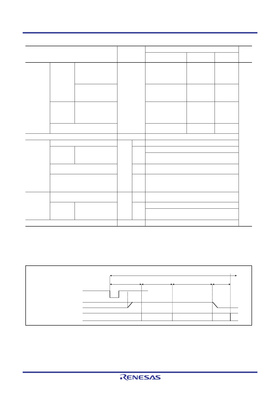
Table 44.10 Times for Conversion during Scanning (in Numbers of Cycles of ADCLK and PCLK)
Note 1. For t
D
, t
DIAG
, t
CONV
, and t
ED
, see Figure 44.22 and Figure 44.23.
Note 2. This is the maximum time required from software writing or trigger input to A/D conversion start.
Note 3. The value is fixed to 0Fh (15 ADCLK) when the temperature sensor output or internal reference voltage is A/D-converted.
Note 4. The required sampling time (ns) is specified according to the voltage conditions. See section 51.5, A/D Conversion
Characteristics.
Note 5. This does not include the time consumed in the path from timer output to trigger input.
Note 6. 2 PCLK + 3 ADCLK when ADCLK is faster than PCLK (PCLK to ADCLK frequency ratio = 1:2 or 1:4).
Figure 44.22 Scan Conversion Timing (Activated by Software or Synchronous Trigger)
Item Symbol
Type/Conditions
UnitSynchronous Trigger
*5
Asynchronous
Trigger
Software
Trigger
Scan start
processing
time*
1,
*
2
A/D
conversion on
group A under
group-A
priority
control.
Group B is to be stopped.
(Group A is activated after
group B is stopped due to
an A/D conversion source
of group A.)
t
D
3 PCLK + 6 ADCLK — — Cycle
Group B is not to be
stopped. (Activation by an
A/D conversion source of
group A.)
2 PCLK + 4 ADCLK — —
A/D
conversion
when self-
diagnosis is
enabled
A/D conversion for self-
diagnosis is to be started.
2 PCLK + 6 ADCLK 4 PCLKB +
6 ADCLK
6 ADCLK
Other than above 2 PCLK + 4 ADCLK 4 PCLKB +
4 ADCLK
4 ADCLK
Disconnection detection assistance processing time t
DIS
The setting of ADNDIS[3:0] (initial value = 00h) × ADCLK*
3
Self-diagnosis
conversion
processing
time*
1
Sampling time t
DIAG
t
SPL
The setting of ADSSTR0 (initial value = 0Dh) × ADCLK*
4
Time for
conversion by
successive
approximation
12-bit conversion accuracy t
SAM
32 ADCLK (during high-speed conversion operation)
41 ADCLK (during low-current conversion operation)
Normal A/D conversion is to be started after
completion of self-diagnosis conversion.
t
DED
2 ADCLK
A/D conversion for self-diagnosis is to be
started after completion of conversion for
continuous scan on the last channel
specified.
t
DSD
2 ADCLK
A/D
conversion
processing
time*
1
Sampling time t
CONV
t
SPL
The setting of ADSSTRn (n = 0 to 7, L, T, O) (initial value =
0Dh) × ADCLK*
4
Time for
conversion by
successive
approximation
12-bit conversion accuracy t
SAM
32 ADCLK (during high-speed conversion operation)
41 ADCLK (during low-current conversion operation)
Scan end processing time*
1
t
ED
1 PCLKB + 3 ADCLK*
6
t
DIAG
t
SCAN
t
CONV
t
ED
DIAG conversion A/D conversion
End
processing
t
D
Software trigger
Synchronous trigger
Waiting
ADST bit
A/D converter

 Loading...


