R01UH0823EJ0100 Rev.1.00 Page 535 of 1823
Jul 31, 2019
RX23W Group 23. Multi-Function Timer Pulse Unit 2 (MTU2a)
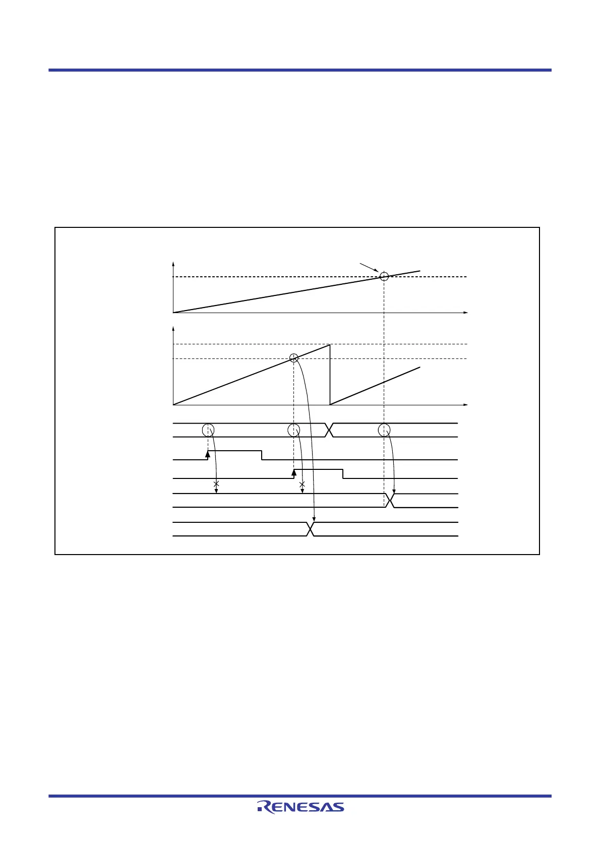
(5) Cascaded Operation Example (d)
Figure 23.24 illustrates the operation when counters MTU1.TCNT and MTU2.TCNT have been cascaded and the
TICCR.I2AE bit has been set to 1 to include the MTIOC2A pin in the MTU1.TGRA input capture conditions. In this
example, the MTU1.TIOR.IOA[3:0] bits have selected occurrence of MTU0.TGRA compare match or input capture for
the input capture timing while the MTU2.TIOR.IOA[3:0] bits have selected the MTIOC2A rising edge for the input
capture timing.
Under these conditions, as the MTU1.TIOR register has selected occurrence of MTU0.TGRA compare match or input
capture for the input capture timing, the MTIOC2A edge is not used for MTU1.TGRA input capture condition although
the TICCR.I2AE bit has been set to 1.
Figure 23.24 Cascaded Operation Example (d)
Time
0513h0512h
0513h
D000h
MTU0.TCNT value
Time
Compare match between MTU0.TCNT and TGRA
MTU2.TCNT value
0000h
0000h
MTU1.TGRA
MTU2.TGRA
MTIOC1A
MTIOC2A
MTU1.TCNT
D000h
FFFFh
MTU0.TGRA