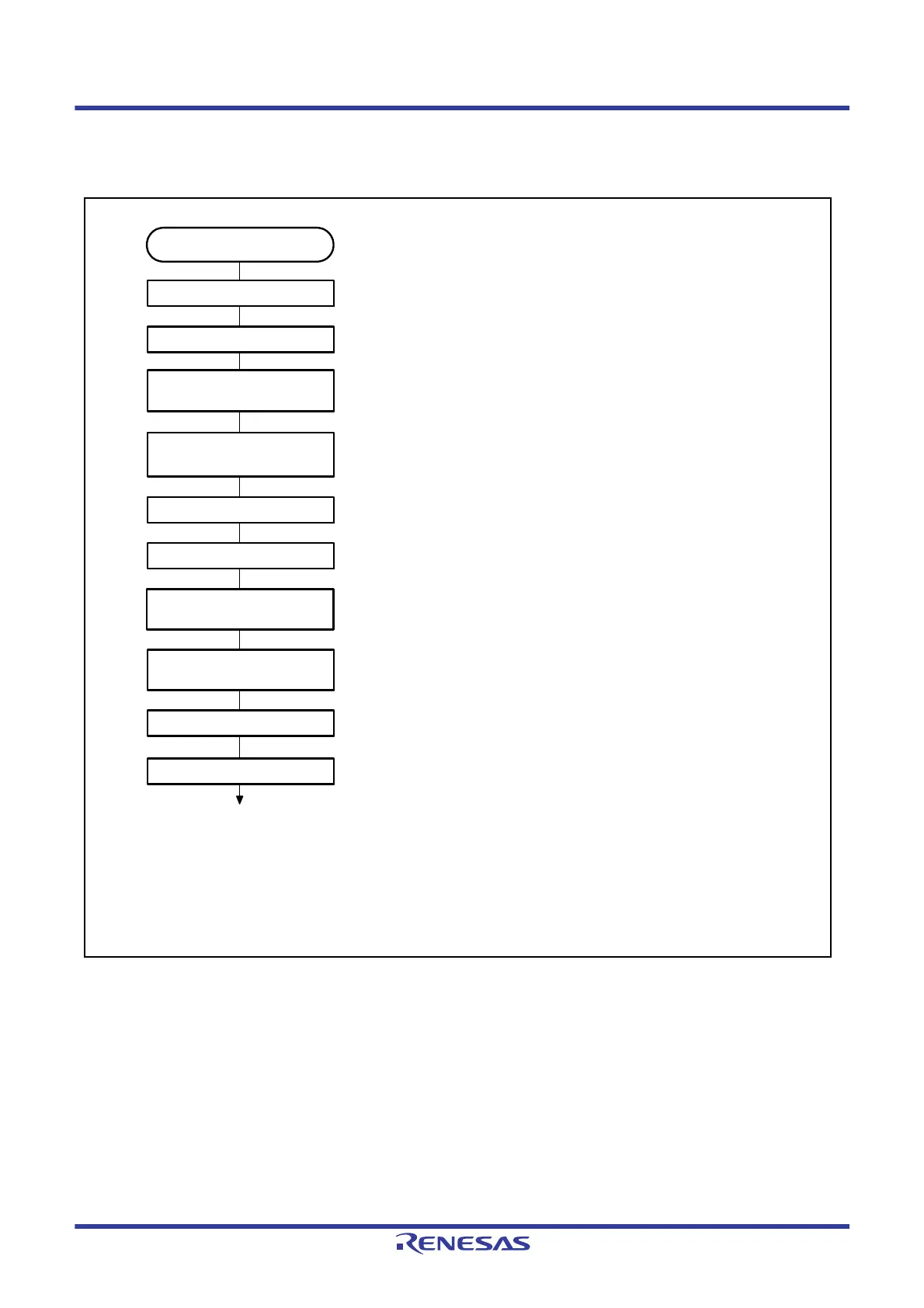
[1] Set the CST3 and CST4 bits in the TSTR register to 0 to stop the
TCNT operation. Specify the reset-synchronized PWM mode while
MTU3.TCNT and MTU4.TCNT are stopped.
[2] Set the Pmn pin function control register and the port I/O register.
[3] Set bits TPSC[2:0] and CKEG[1:0] in the MTU3.TCR register to
select the count clock source and clock edge for MTU3. Set the
MTU3.TCR.CCLR[2:0] bits to select TGRA compare-match as a
counter clear source.
[4] When performing brushless DC motor control, set the TGCR.BDC
bit and set the feedback signal input source and output chopping or
gate signal direct output.
[5] Set counters MTU3.TCNT and MTU4.TCNT to 0000h.
[6] The MTU3.TGRA register is the cycle register. Set the waveform
cycle value in the MTU3.TGRA register. Set the transition timing of
the PWM output waveforms in registers MTU3.TGRB,
MTU4.TGRA, and MTU4.TGRB. Set times within the compare
match range of the MTU3.TCNT counter.
X ≤ MTU3.TGRA (X: Setting value)
[7] Enable or disable toggle output synchronized with the PWM cycle
using the TOCR1.PSYE bit, and set the PWM output level with bits
OLSP and OLSN. When specifying the PWM output Level. In buffer
operation of registers TOCR2 and TOLBR, refer to Figure 23.3.
[8] Set the MTU3.TMDR.MD[3:0] bits to 1000b to select the reset-
synchronized PWM mode. Set the BFA bit to 1 for buffer operation
of registers TGRA and TGRC, and the BFB bit to 1 for buffer
operation of registers TGRB and TGRD, if necessary.
Set the initial value in the MTU4.TMDR register.
[9] Set the enabling/disabling of the PWM waveform output pin in the
TOER register.
[10] Set the TSTR.CST3 bit to 1 to start the count operation.
Note: The output waveform starts to toggle at the point of MTU3.TCNT =
MTU3.TGRA = X by setting X = MTU3.TGRA, i.e., cycle = duty cycle.

 Loading...


