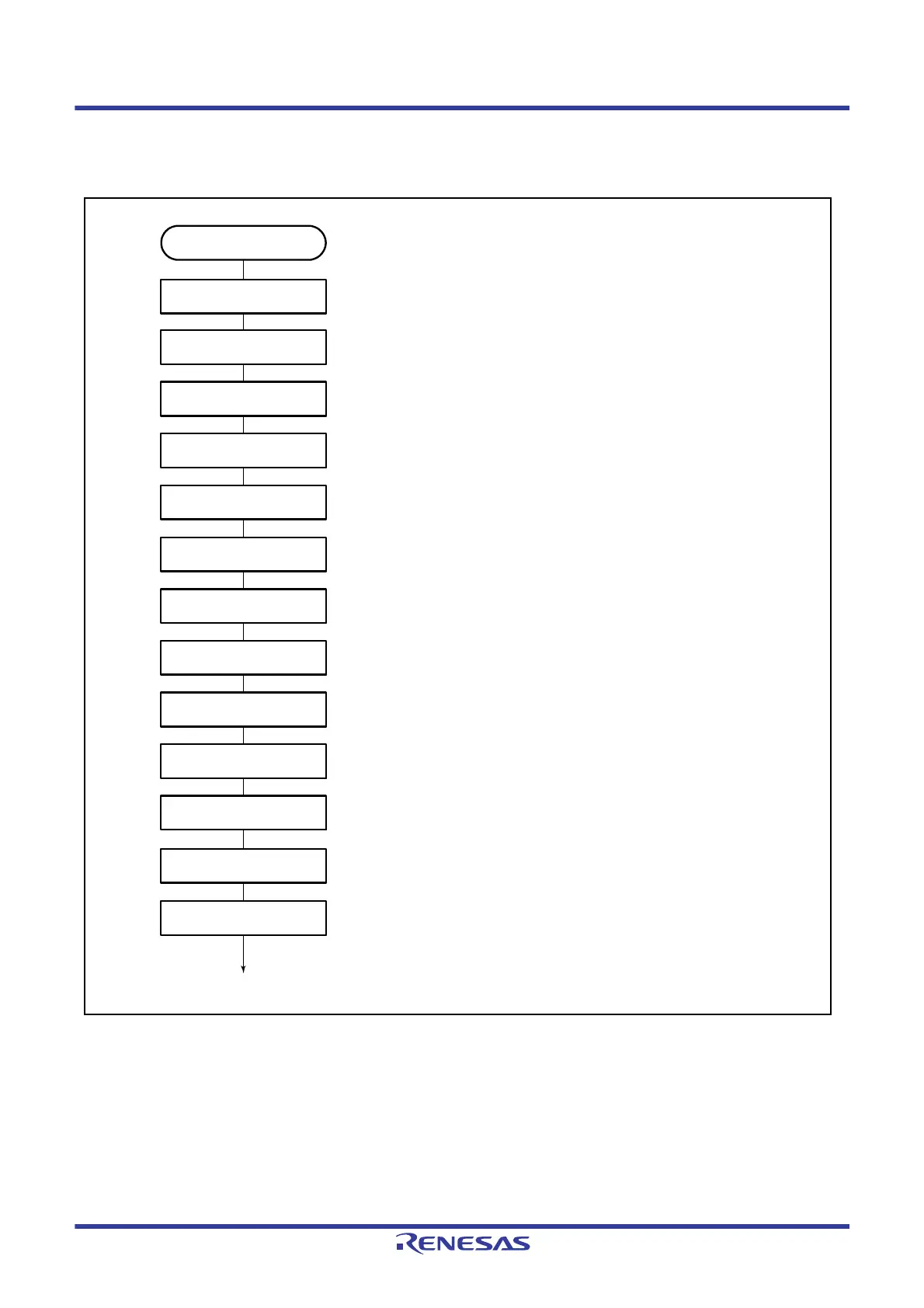
[1] Set bits CST3 and CST4 in the TSTR register to 0 to stop TCNT operation.
Specify complementary PWM mode while counters MTU3.TCNT and
MTU4.TCNT are stopped.
[2] Set the Pmn pin function control register and the port I/O register.
[3] Set the same count clock source and clock edge for MTU3 and MTU4 with
bits TPSC[2:0] and bits CKEG[1:0] in the TCR register. Use the CCLR[2:0]
bits to set synchronous clearing only when restarting by synchronous
clearing with another channel during complementary PWM mode operation.
[4] When performing brushless DC motor control, set TGCR.BDC bit and set
the feedback signal input source and output chopping or gate signal direct
output.
[5] Set the dead time in the MTU3.TCNT counter. Set the MTU4.TCNT counter
to 0000h.
[6] Set only when restarting by synchronous clearing with another channel
during complementary PWM mode operation. In this case, synchronize the
channel generating the synchronous clear with MTU3 and MTU4 using the
TSYR register.
[7] Set the output PWM duty cycles in the compare registers (MTU3.TGRB,
MTU4.TGRA, and MTU4.TGRB) and buffer registers (MTU3.TGRD,
MTU4.TGRC, and MTU4.TGRD). Set the same value in the buffer registers
and the compare registers.
[8] This setting is necessary only when no dead time should be generated.
Make appropriate settings in the TDER register so that no dead time is
generated.
[9] Set the dead time in the TDDR register, 1/2 the carrier cycle in the TCDR
register and TCBR register, and 1/2 the carrier cycle plus the dead time in
registers MTU3.TGRA and MTU3.TGRC. When no dead time generation is
selected, set 1 in the TDDR register and 1/2 the carrier cycle + 1 in registers
MTU3.TGRA and MTU3.TGRC.
[10] Enable or disable toggle output synchronized with the TOCR1.PSYE bit,
and set the PWM output level with bits OLSP and OLSN.
When specifying the PWM output level by using the TOLBR register as a
buffer for the MTU.TOCR2 register, refer to Figure 23.3, Example of PWM
Output Level Setting Procedure in Buffer Operation.
[11] Select complementary PWM mode in the MTU3.TMDR register. Set the
BFA bit to 1 for buffer operation of registers TGRA and TGRC, and the BFB
bit to 1 for buffer operation of registers TGRB and TGRD, if necessary. Do
not set the MTU4.TMDR register.
[12] Set enabling/disabling of PWM waveform output pin output in the TOER
register.
[13] Set bits CST3 and CST4 in the TSTR register to 1 simultaneously to start
the count operation.

 Loading...


