Chapter 7 387
ADC/Interface Section
A3 Assembly Control Circuits
7. Monitor A3U401 pin 3 (LR_STB) with an oscilloscope or logic probe.
This is the strobe for the A15 RF assembly.
8. Press AUX CTRL and REAR PANEL and check that pulses occur when
toggling between
10 MHz INT and 10 MHz EXT.
9. Monitor A3U401 pin 5 (LF_STB) with an oscilloscope or logic probe.
This is the strobe for the A14 frequency control assembly.
10.Press
AMPLITUDE and check that pulses occur when toggling
between
ATTEN settings of 10 and 20 dB.
11.Monitor A3U401 pin 7 (LI_STB) with an oscilloscope or logic probe.
This is the strobe for the A5 IF assembly.
12.Press
AMPLITUDE and check that pulses occur when toggling
between
REF LVL settings of −10 dBm and −20 dBm.
13.Monitor A3U401 pin 9 (LV_STB) with an oscilloscope or logic probe.
This is the strobe for the A4 log amplifier/cal oscillator assembly.
14.Press
AMPLITUDE and check that pulses occur when toggling
between
LINEAR and LOG DB/DIV.
Interface Strobe Select
Refer to function block K of A3 Interface Assembly Schematic Diagram
(sheet 3 of 6) in the
HP 8560 E-Series Spectrum Analyzer Component Level
Information.
Interface strobe select generates the various strobes used by circuits on
the A3 Interface Assembly. Table 7-10 on page 387 and Table 7-11 on
page 388 are the truth tables for demultiplexers A3U410 and A3U500.
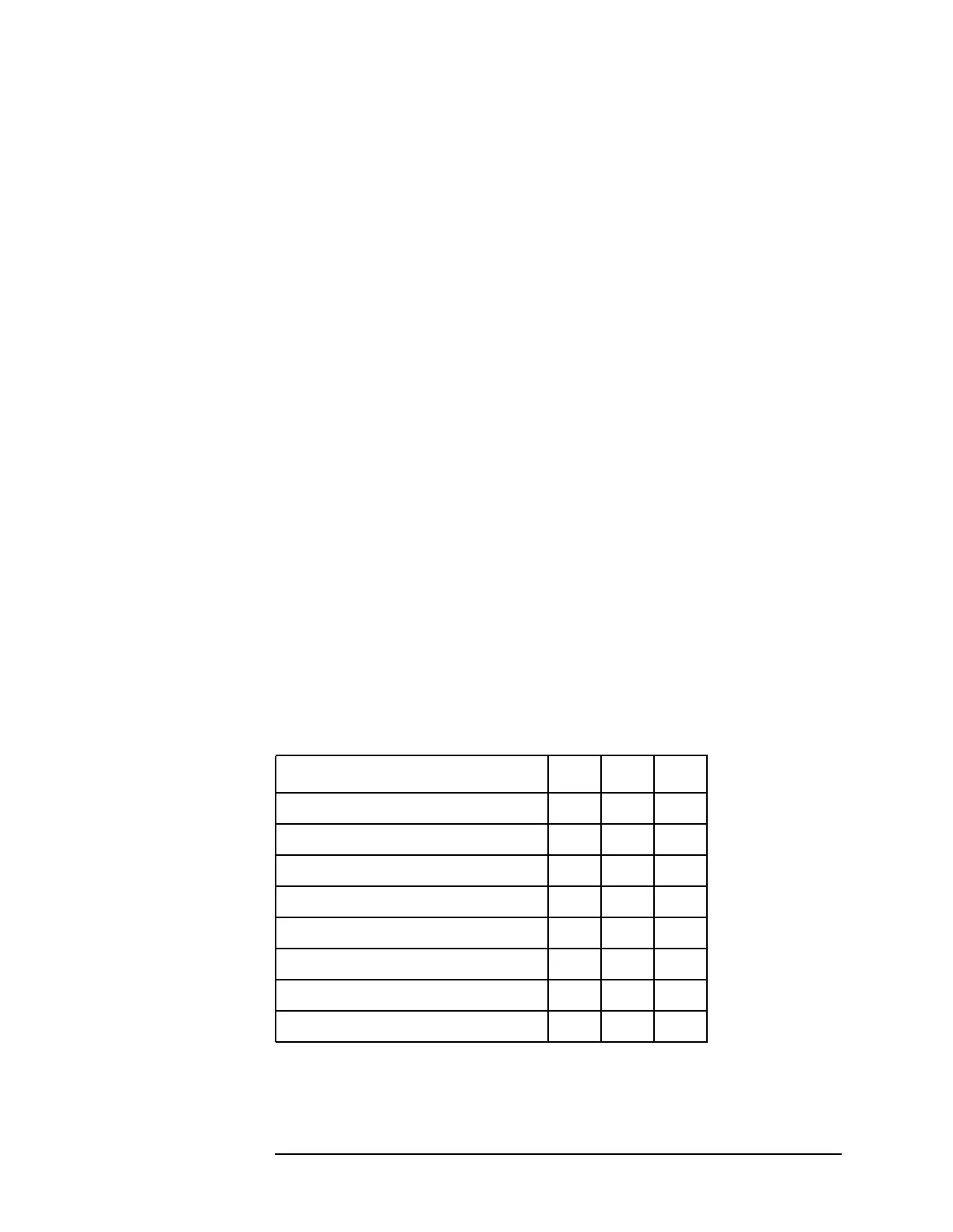
Table 7-10 Demultiplexer A3U410 Truth Table
Selected Output Line IA1 IA2 IA3
Pin 15, LSCAN_KBD L L L
Pin 14, LDACU1 H L L
Pin 13, LDAC1 L H L
Pin 12, LDAC2 H H L
Pin 11, LDAC3 L L H
Pin 10 H L H
Pin 9, LTIMER L H H
Pin 7, LADC_REG1 H H H

 Loading...


