Chapter 7 397
ADC/Interface Section
A16 Assembly Fast ADC Control Circuits (8560E with Option 007)
Reference Clock
Refer to function block B of the A16 fast ADC assembly schematic
diagram in the HP 8560 E-Series Component Level Information.
The reference clock circuitry takes the 8 MHz CMOS square wave clock
from the A2 controller assembly (via W59, coax 839) and triples the
frequency to 24 MHz. Inverters U5A and U5B provide the proper match
for the 8 MHz clock input, and also the desired drive level into the 24
MHz bandpass filter. The 24 MHz bandpass filter consists of R5, C8, L1,
C9, C10, L2, C11, L3, C12, L4, C13, C14, and R6. Inverters U6A and
U6B provide amplification of the 24 MHz clock to produce CMOS levels,
and also buffer the 24 MHz clock output.
Clock and Sample Rate Generator
Refer to function block C of the A16 fast ADC assembly schematic
diagram in the HP 8560 E-Series Component Level Information.
The clock and sample rate generator takes the 24 MHz reference clock
signal and generates all of the various clock signals used on the A16
fast ADC assembly. The sample rate generator consists of CMOS latch
U15, CMOS counters U14 and U16, and CMOS flip-flops U7B and U9A.
The sample rate generator only controls the rate at which the static
RAM address counter (15-bit circular address counter) and the 16-bit
post-trigger counter are clocked (ACLK and PCLK respectively). The
sample rate generator also controls the number of flash ADC samples
taken per bucket. The range of the sample rate is 1 sample per bucket
(12 MHz rate) to 256 samples per bucket (less than 12 MHz rate).
SCLK-1 is an input to PAL U1 (block A) and affects the LP/Q signal to
ensure that the first sample of a bucket is always clocked into latch U30
(block J) and written into static RAM U32 (block K) when the detection
mode is peak or pit and the sample rate is less than 12 MHz. Refer to
Table 7-12, LP/Q Truth Table in this chapter.
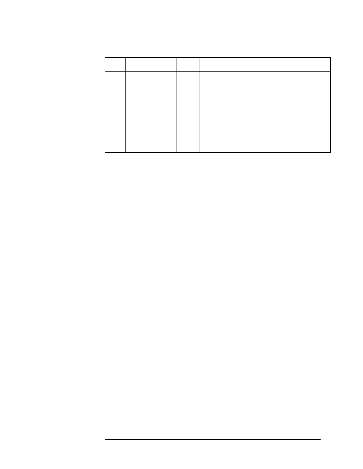
Bit
15
LPEAK Peak/pit detection mode control.
1 Enables pit (negative-peak) detectionmode if
LSAMPLE (Bit 4) is also high.
0 Enables peak detection mode if LSAMPLE
(Bit 4) is high.
Table 7-13 Control Word at Primary Address (U3 and U4)
Bit Mnemonic State Description

 Loading...


