Zynq-7000 AP SoC and 7 Series FPGAs MIS v4.1 114
UG586 November 30, 2016
www.xilinx.com
Chapter 1: DDR3 and DDR2 SDRAM Memory Interface Solution
Table 1-48 describes the register bit usage when DQ_WIDTH = 72.
Table 1-49 describes the register bit usage when DQ_WIDTH = 144.
User Interface Block
The UI block presents the UI to a user design. It provides a simple alternative to the native
interface. The UI block:
• Buffers read and write data
• Reorders read return data to match the request order
• Presents a flat address space and translates it to the addressing required by the SDRAM
Native Interface
The native interface connects to an FPGA user design to allow access to an external memory
device.
Command Request Signals
The native interface provides a set of signals that request a read or write command from the
Memory Controller to the memory device. These signals are summarized in Table 1-50.
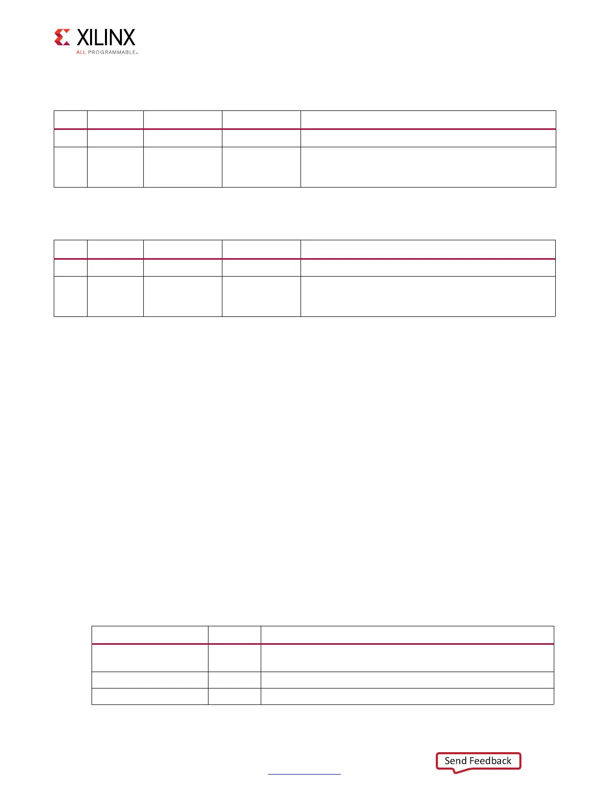
Table 1-48: Fault Injection ECC Register Bit Definitions for 72-Bit External Memory Width
Bits Name Core Access Reset Value Description
31:8 Reserved RSVD – Reserved
7:0 FI_ECC W 0
Bit positions set to 1 toggle the corresponding bit of the
next ECC written to the memory. The register is
automatically cleared after the fault has been injected.
Table 1-49: Fault Injection ECC Register Bit Definitions for 144-Bit External Memory Width
Bits Name Core Access Reset Value Description
31:16 Reserved RSVD – Reserved
15:0 FI_ECC W 0
Bit positions set to 1 toggle the corresponding bit of the
next ECC written to the memory. The register is
automatically cleared after the fault has been injected.
Table 1-50: Native Interface Command Signals
Signal Direction Description
accept Output
This output indicates that the memory interface accepts the
request driven on the last cycle.
bank[2:0] Input This input selects the bank for the current request.
bank_mach_next[] Output This output is reserved and should be left unconnected.