Zynq-7000 AP SoC and 7 Series FPGAs MIS v4.1 348
UG586 November 30, 2016
www.xilinx.com
Chapter 2: QDR II+ Memory Interface Solution
DCI (HP banks) or IN_TERM (HR banks) is required at the FPGA to meet the specified
performance. Designs generated by the MIG tool use the DCI standards for Data Read (Q)
and Read Clock (CQ_P and CQ_N) in the High-Performance banks. In the High-Range banks,
the MIG tool uses the HSTL_I standard with the internal termination (IN_TERM) attribute
chosen in the GUI.
Clocking
The 7 series FPGA MIG QDR II+ SRAM design has two clock inputs, the reference clock and
the system clock. The reference clock drives the IODELAYCTRL components in the design,
while the system clock input is used to create all MIG design clocks that are used to clock
the internal logic, the frequency reference clocks to the phasers, and a synchronization
pulse required for keeping PHY control blocks synchronized in multi-I/O bank
implementations. For more information on clocking architecture, see Clocking Architecture,
page 322.
The MIG tool allows you to input the Memory Clock Period and then lists available Input
Clock Periods that follow the supported clocking guidelines. Based on these two clock
periods selections, the generated MIG core appropriately sets the PLL parameters. The MIG
tool enables automatic generation of all supported clocking structures. For information on
how to use the MIG tool to set up the desired clocking structure including input clock
placement, input clock frequency, and IDELAYCTRL ref_clk generation, see Creating the 7
Series FPGA QDR II+ SRAM Design, page 287.
Input Clock Guidelines
IMPORTANT: The input system clock cannot be generated internally.
• PLL Guidelines
°
CLKFBOUT_MULT_F (M) must be between 1 and 16 inclusive.
°
DIVCLK_DIVIDE (D, Input Divider) can be any value supported by the PLLE2
parameter.
°
CLKOUT_DIVIDE (O, Output Divider) must be 2 for 400 MHz and up operation and 4
for below 400 MHz operation.
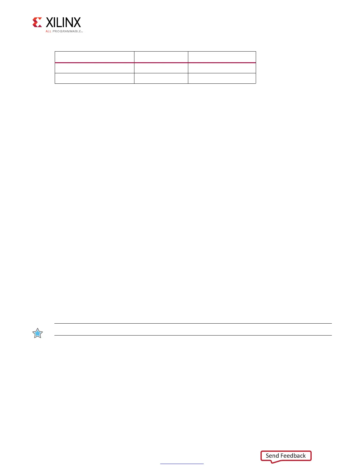
qdr_sa Output HSTL_I
qdr_w_n Output HSTL_I
Notes:
1. All signals operate at 1.5V.
Table 2-14: I/O Standards (Cont’d)
Signal
(1)
Direction I/O Standard
 Loading...


