Zynq-7000 AP SoC and 7 Series FPGAs MIS v4.1 40
UG586 November 30, 2016
www.xilinx.com
Chapter 1: DDR3 and DDR2 SDRAM Memory Interface Solution
The desired input clock period is selected from the list. These values are determined by the
memory clock period chosen and the allowable limits of the parameters. See Design
Guidelines, page 192 for more information on the PLL parameter limits.
Select Additional Clocks option appears for AXI interface designs only. Selection is
allowed for up to five additional clocks which are generated from the same MMCM that
generates UI_CLK.
IMPORTANT: The Select Additional Clocks option appears in Vivado IP integrator flow only.
Click Next to display the FPGA Options page.
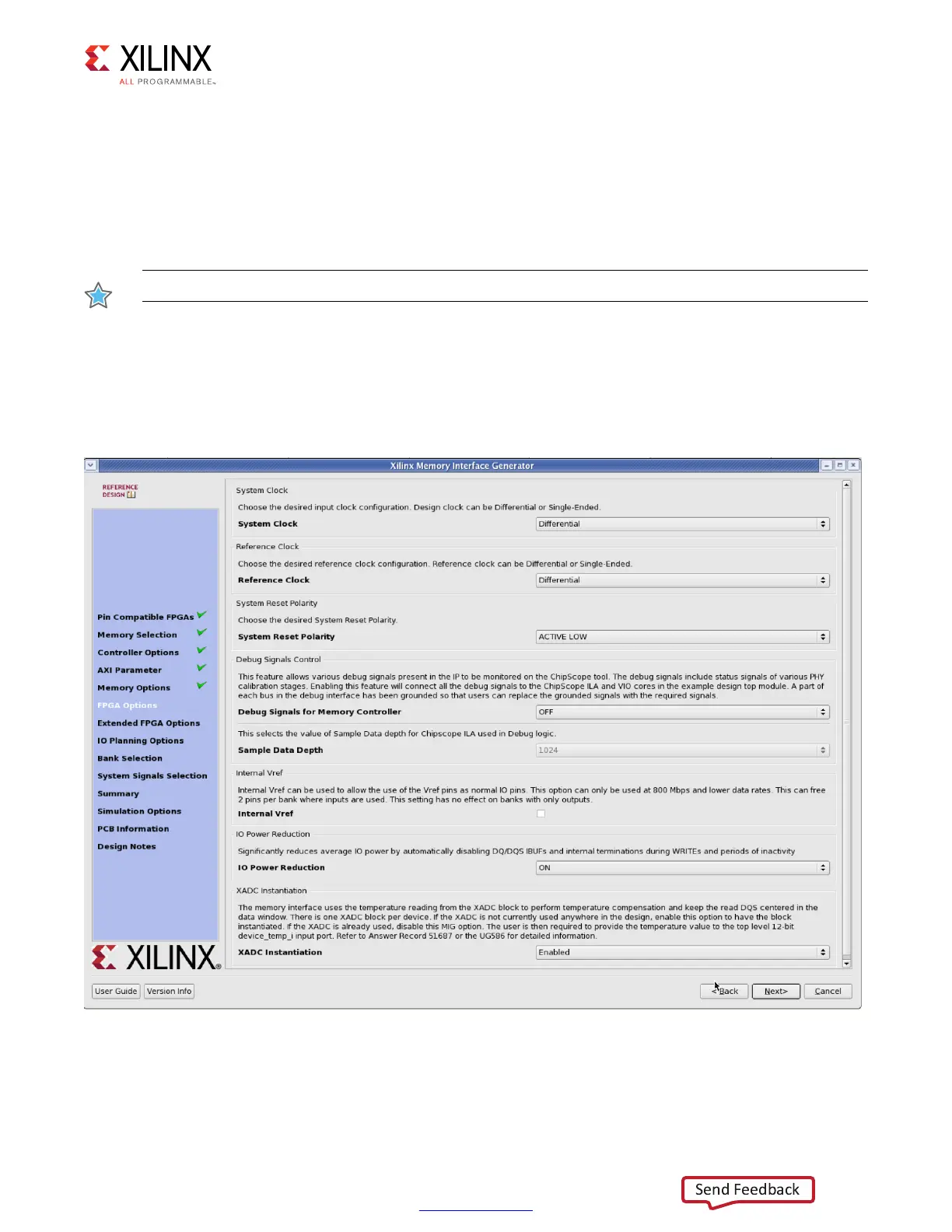
FPGA Options
Figure 1-22 shows the FPGA Options page.
X-Ref Target - Figure 1-22
Figure 1-22: FPGA Options
 Loading...


