Zynq-7000 AP SoC and 7 Series FPGAs MIS v4.1 611
UG586 November 30, 2016
www.xilinx.com
Chapter 4: LPDDR2 SDRAM Memory Interface Solution
Designing with the Core
The core is bundled with an example design that can be simulated. The example design can
be used as a starting point for the user design or as a reference for debugging purposes.
Only supported modifications should be made to the configuration of the core. See
Customizing the Core, page 621 for supported configuration parameters.
Interfacing to the Core
The Memory Controller can be connected using either the UI or the native interface. The UI
resembles a simple FIFO interface and always returns the data in order. The native interface
offers higher performance in some situations, but is more challenging to use.
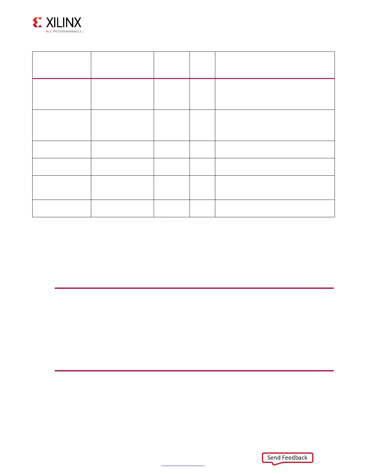
phy_mc_cmd_full 1 Output
Active-
High
Bitwise OR of all the Almost FULL flags of all
the command OUT_FIFOs. The Almost FULL
flag is asserted when the FIFO is one entry
away from being FULL.
phy_mc_data_full 1 Output
Active-
High
Bitwise OR of all the Almost FULL flags of all
the write data OUT_FIFOs. The Almost FULL
flag is asserted when the FIFO is one entry
away from being FULL.
phy_rd_data
[2 × nCK_PER_CLK ×
DQ_WIDTH – 1:0]
Output –
This is the read data from the dedicated
PHY. It is 4x the memory DQ width.
phy_rddata_valid 1 Output
Active-
High
This signal is asserted when valid read data
is available.
calib_rd_data_offset [6 × RANKS – 1:0] Output –
This signal is the calibrated read data offset
value with respect to command 0 in the
sequence of four commands.
init_calib_complete 1 Output
Active-
High
This signal is asserted after memory
initialization and calibration are completed.
Notes:
1. The parameter nCK_PER_CLK defines the number of LPDDR2 SDRAM clock cycles per PHY_Clk cycle.
2. The parameter ROW_WIDTH is the number of LPDDR2 SDRAM ranks.
3. The parameter BANK_WIDTH is the number of LPDDR2 SDRAM banks.
4. The parameter CS_WIDTH is the number of LPDDR2 SDRAM cs_n signals.
5. The parameter CKE_WIDTH is the number of LPDDR2 SDRAM CKE signals.
6. The parameter DQ_WIDTH is the width of the LPDDR2 SDRAM DQ bus.
Table 4-24: Memory Controller to Calibration Logic Interface Signals (Cont’d)
Signal Name Width
I/O
To/From
PHY
Type Description
 Loading...


