EasyManua.ls Logo

Xilinx Zynq-7000 User Manual

Xilinx Zynq-7000
678 pages
To Next Page IconTo Next Page
To Previous Page IconTo Previous Page
Page #492 background imageLoading...
Page #492 background image
Zynq-7000 AP SoC and 7 Series FPGAs MIS v4.1 492
UG586 November 30, 2016
www.xilinx.com
Chapter 3: RLDRAM II and RLDRAM 3 Memory Interface Solutions
Memory Initialization
For simulation, the MIG tool sets up the design parameters such that long wait times usually
required for memory initialization are skipped. These parameters can result in memory
model warnings. For the design to properly initialize and calibrate the full memory array in
hardware, the top-level MIG tool design file (example_top.v) cannot use any abbreviated
value for these parameters. The MIG tool output properly sets the abbreviated values in the
test bench and the full range values in the top-level design module.
Calibration
Calibration completes read leveling and read enable calibration. This is completed over
three stages. This sequence successfully completes when the init_calib_complete
signal is asserted. For more details, see Physical Interface, page 436.
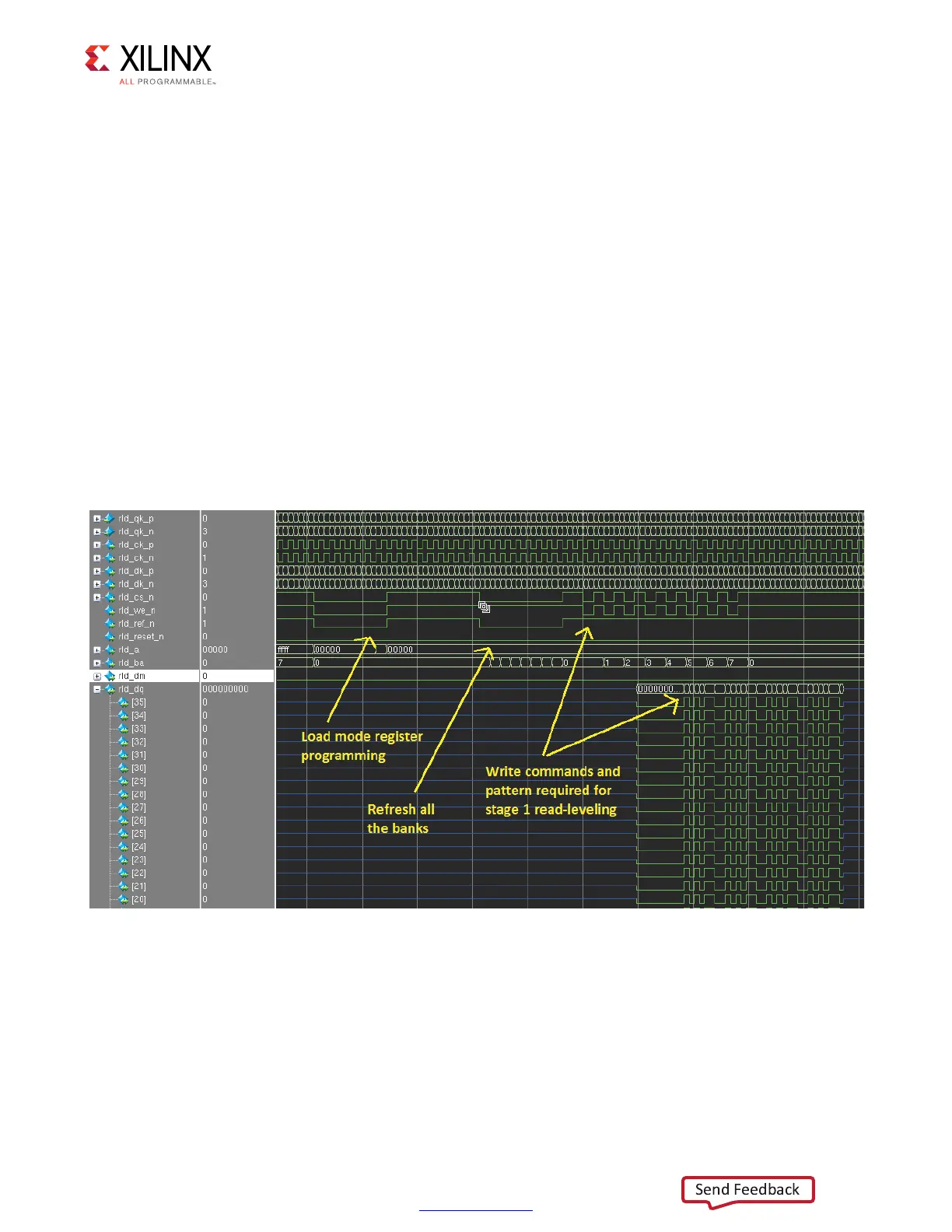
The first stage performs per-bit read leveling calibration. The data pattern used during this
stage is 0_F_0_F_0_F_F_0. The data pattern is first written to the memory, as shown in
Figure 3-69.
X-Ref Target - Figure 3-69
Figure 3-69: Writes for First Stage Read Calibration
Send Feedback

Table of Contents

Other manuals for Xilinx Zynq-7000

Question and Answer IconNeed help?

Do you have a question about the Xilinx Zynq-7000 and is the answer not in the manual?

Xilinx Zynq-7000 Specifications

General IconGeneral
SeriesZynq-7000
Number of CoresDual-core
Processor SpeedUp to 1 GHz
Device TypeSoC
Logic CellsUp to 350K
DSP SlicesUp to 900
External Memory InterfacesDDR3, DDR2, LPDDR2
I/O StandardsLVCMOS, HSTL, SSTL
Operating Temperature-40°C to +100°C (Industrial), 0°C to +85°C (Commercial)
Package OptionsVarious BGA packages
I/O Voltage3.3V

Summary

Chapter 1: DDR3 and DDR2 SDRAM Memory Interface Solution

Introduction

Overview of the DDR3 and DDR2 SDRAM Memory Interface Solution, its architecture, and features.

Features

Highlights enhancements in 7 series FPGA memory interface solutions over earlier families.

Chapter 2: QDR II+ Memory Interface Solution

Introduction

Details the QDR II+ SRAM Memory Interface Solution, its architecture, and usage.

Chapter 3: RLDRAM II and RLDRAM 3 Memory Interface Solutions

Introduction

Explains RLDRAM II/III Memory Interface Solutions, covering architecture, usage, and simulation.

Chapter 4: LPDDR2 SDRAM Memory Interface Solution

Introduction

Introduces the LPDDR2 SDRAM Memory Interface Solution, its core components, and features.

Features

Details enhancements in LPDDR2 SDRAM solutions, including performance and hardware blocks.

Chapter 5: Multicontroller Design

Introduction

Describes specifications, supported features, and pinout rules for multicontroller designs.

Chapter 6: Upgrading the ISE/CORE Generator MIG Core in Vivado

Appendix A: General Memory Routing Guidelines

Related product manuals