Zynq-7000 AP SoC and 7 Series FPGAs MIS v4.1 154
UG586 November 30, 2016
www.xilinx.com
Chapter 1: DDR3 and DDR2 SDRAM Memory Interface Solution
Implementation Details
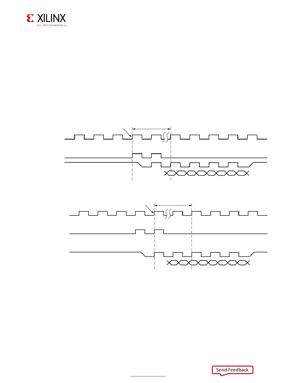
A write command is issued with a known write data pattern (FF 00 AA 55 55 AA 99 66)
to a specific location. This is followed by a read command to the same location. The data
read back out of the IN_FIFO is compared with the expected data pattern on a byte basis. If
the data read out matches the expected pattern, no further changes are required in the
write path for that byte, as shown in Figure 1-69. If the first two data words read back match
the second set of data words in the expected pattern, the DQS and DQ 3-state signal must
be delayed by one memory clock. This scenario is shown in Figure 1-70. After all the bytes
are calibrated, the calibration logic asserts the init_calib_complete signal indicating
the completion of the initialization and calibration sequence. The Memory Controller can
now drive the address, command, and data buses.
Read Leveling
Read leveling stage 1 is required to center align the read strobe in the read valid data
window for the first stage of capture. In strobe-based memory interfaces like DDR2 or
DDR3 SDRAM, the second stage transfer requires an additional pulse which in
7 series FPGAs is provided by the PHASER_IN block. This stage of calibration uses the
PHASER_IN stage 2 fine delay line to center the capture clock in the valid DQ window. The
capture clock is the free-running FREQ_REF clock that is phase aligned to read DQS in the
PHASER_IN phase locked stage.
X-Ref Target - Figure 1-69
Figure 1-69: DQS Aligned to the Correct CK Edge – No Change in Write Path
5'?C??
#+ COMP
$1 COMP
7RITELEVELED
$13 #OMP
ALIGNEDTOTHE
7R?#MD#+EDGE
&& !! !!
#,7
#+EDGETHATCLOCKS7R?#MD
X-Ref Target - Figure 1-70
Figure 1-70: DQS Aligned to Incorrect CK Edge – Delay DQS/DQ by One Memory Clock Cycle
5'?C??
#+ COMP
7RITELEVELED
$13 COMP
ONECYCLEEARLIERTHAN
7R?#MD#+EDGE
$13 COMP
MUSTBEDELAYEDBY
MEMORYCLOCKCYCLE
&& !! !!
#7,
#+EDGETHATCLOCKS7R?#MD
 Loading...


