Zynq-7000 AP SoC and 7 Series FPGAs MIS v4.1 166
UG586 November 30, 2016
www.xilinx.com
Chapter 1: DDR3 and DDR2 SDRAM Memory Interface Solution
Example (2) – When the selected option in the MIG GUI is ROW_BANK_COLUMN and the
address to the controller is mapped accordingly.
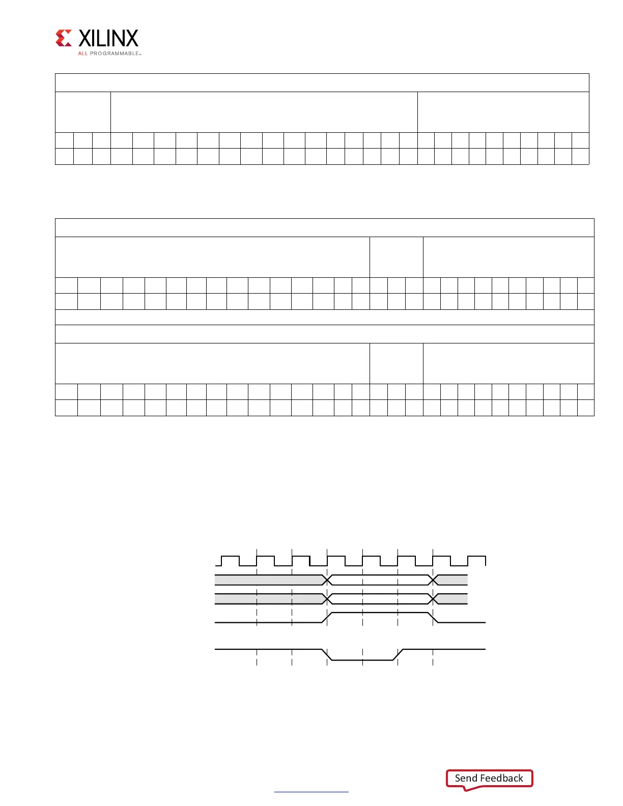
Command Path
When the user logic app_en signal is asserted and the app_rdy signal is asserted from the
UI, a command is accepted and written to the FIFO by the UI. The command is ignored by
the UI whenever app_rdy is deasserted. The user logic needs to hold app_en High along
with the valid command and address values until app_rdy is asserted as shown in
Figure 1-74.
BANK
Address
Bits
ROW Address Bits COLUMN Address Bits
2726252423222120191817161514131211109876543210
R0 C9 C8 R4 R3 B2 B1 B0 R14R13R12R11R10R9 R8 C7 C6C5 R2R1R7R6R5C4C3C2C1C0
Original Mapping of the Address Bits
Original Mapping of the Address Bits
ROW Address Bits
BANK
Address
Bits
COLUMN Address Bits
2726 252423222120191817161514131211109876543210
R14R13 R12R11R10R9 R8 R7 R6 R5 R4 R3 R2 R1R0B2 B1B0 C9C8C7C6C5C4C3C2C1C0
Remapped Address with TG_TEST
ROW Address Bits
BANK
Address
Bits
COLUMN Address Bits
2726 252423222120191817161514131211109876543210
R0 C9 C8 R4 R3 B2 B1 B0 R14R13R12R11R10R9R8C7C6C5R2R1R7R6R5C4C3C2C1C0
X-Ref Target - Figure 1-74
Figure 1-74: UI Command Timing Diagram with app_rdy Asserted
5'?C??
CLK
APP?CMD
72)4%
APP?ADDR
!DDR
APP?EN
APP?RDY
#OMMANDISACCEPTEDWHENAPP?RDYIS(IGHANDAPP?ENIS(IGH
 Loading...


