Zynq-7000 AP SoC and 7 Series FPGAs MIS v4.1 165
UG586 November 30, 2016
www.xilinx.com
Chapter 1: DDR3 and DDR2 SDRAM Memory Interface Solution
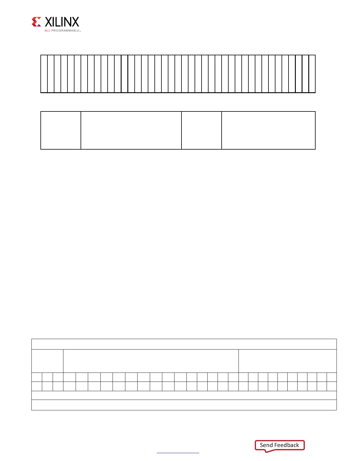
Figure 1-72 and Figure 1-73 show that the address map is controlled by the string
parameter MEM_ADDR_ORDER. This parameter can take the following values:
• BANK_ROW_COLUMN – Address map is as shown in Figure 1-72.
• ROW_BANK_COLUMN – Address map is as shown in Figure 1-73.
• TG_TEST – Address map is used for testing purpose only. It enables the address remap
to test address access to different portions of the DRAM. It remaps the address as
explained in the following examples. The remap is done within the UI portion of the
controller.
Note:
The row width, column width, and bank width value settings are assumed for the following
examples:
°
Row Width – 15
°
Bank Width – 3
°
Column Width – 10
Example (1) – When the selected option in the MIG GUI is BANK_ROW_COLUMN and the
address to the controller is mapped accordingly.
X-Ref Target - Figure 1-73
Figure 1-73: Memory Address Mapping for Row-Bank-Column Mode in UI Module
5SER!DDRESS
!
N
!
!
!
!
!
!
-EMORY
2ANK 2OW "ANK #OLUMN
5'?C?A?
Original Mapping of the Address Bits
BANK
Address
Bits
ROW Address Bits COLUMN Address Bits
2726252423222120191817161514131211109876543210
B2 B1 B0 R14R13R12R11R10R9 R8 R7 R6 R5 R4 R3 R2 R1 R0 C9C8C7C6C5C4C3C2C1C0
Remapped Address with TG_TEST
 Loading...


