Zynq-7000 AP SoC and 7 Series FPGAs MIS v4.1 588
UG586 November 30, 2016
www.xilinx.com
Chapter 4: LPDDR2 SDRAM Memory Interface Solution
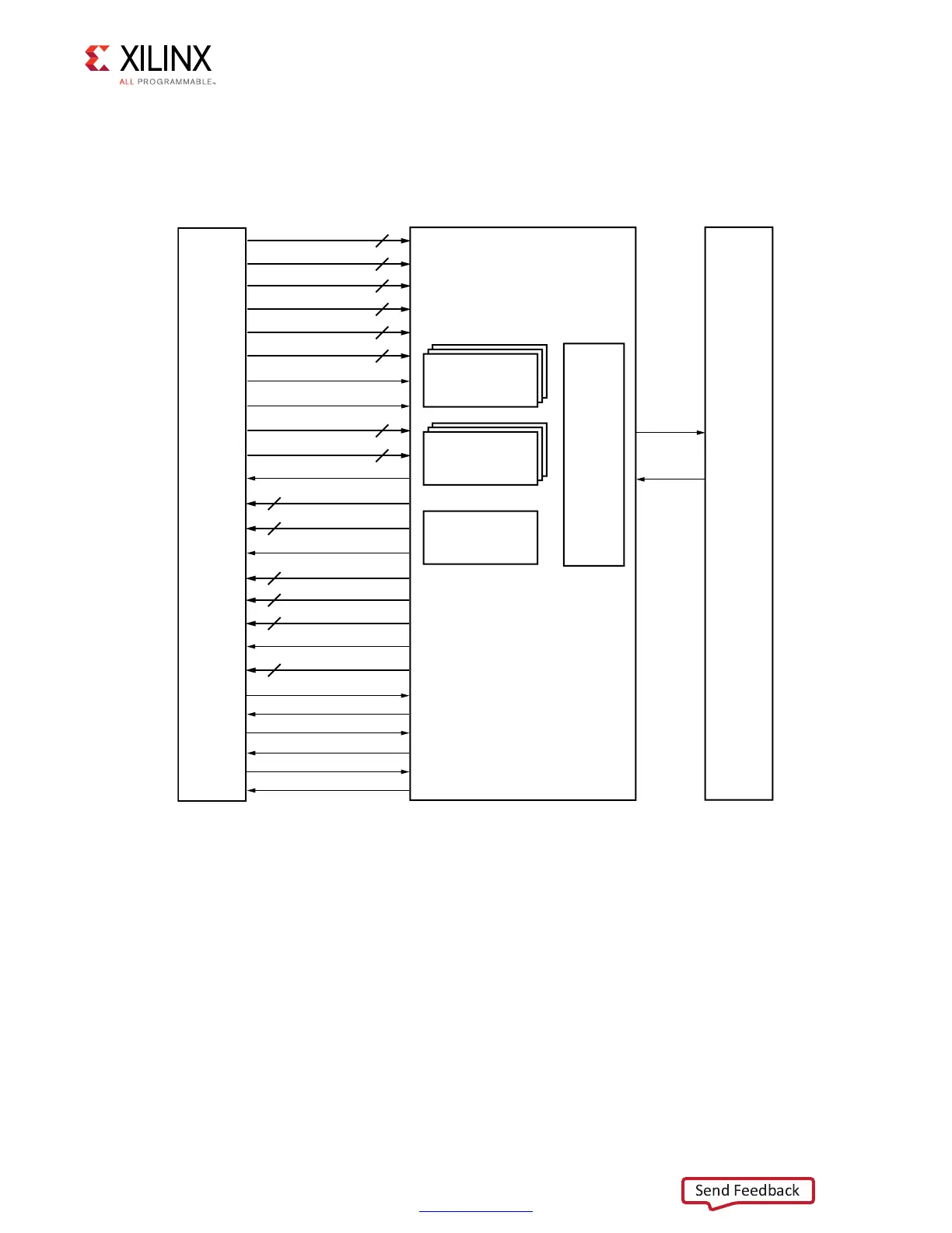
Memory Controller
In the core default configuration, the Memory Controller (MC) resides between the UI block
and the physical layer. This is depicted in Figure 4-46.
The Memory Controller is the primary logic block of the memory interface. It receives
requests from the UI and stores them in a logical queue. Requests are optionally reordered
to optimize system throughput and latency.
The Memory Controller block is organized as four main pieces:
• Configurable number of “bank machines”
• Configurable number of “rank machines”
• Column machine
• Arbitration block
X-Ref Target - Figure 4-46
Figure 4-46: Memory Controller
RANK
BANK
ROW
COL
CMD
DATA?BUF?ADDR
HI?PRIORITY
USE?ADDR
WR?DATA
WR?DATA?MASK
ACCEPT
BANK?MACH?NEXT
WR?DATA?ADDR
WR?DATA?EN
WR?DATA?OFFSET
RD?DATA
RD?DATA?ADDR
RD?DATA?EN
RD?DATA?OFFSET
2ANK-ACHINES
"ANK-ACHINES
!RBITER
-#0(9
)NTERFACE
0HYSICAL
,AYER
5SER
)NTERFACE
"LOCK
#OLUMN-ACHINE
5'?C??
APP?SR?REQ
APP?SR?ACTIVE
APP?REF?REQ
APP?REF?ACK
APP?ZQ?REQ
APP?ZQ?ACK
 Loading...


