Zynq-7000 AP SoC and 7 Series FPGAs MIS v4.1 44
UG586 November 30, 2016
www.xilinx.com
Chapter 1: DDR3 and DDR2 SDRAM Memory Interface Solution
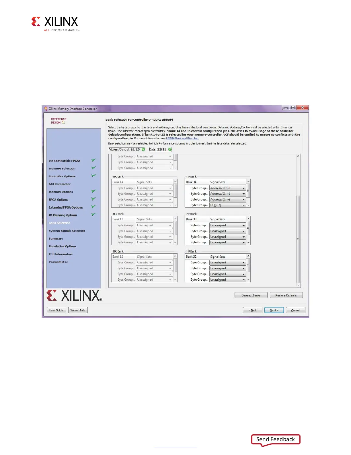
Bank Selection
This feature allows the selection of bytes for the memory interface. Bytes can be selected
for different classes of memory signals, such as:
• Address and control signals
• Data signals
For customized settings, click Deselect Banks and select the appropriate bank and memory
signals. Click Next to move to the next page if the default setting is used.
To unselect the banks that are selected, click Deselect Banks. To restore the defaults, click
Restore Defaults.
VCCAUX_IO groups are shown for HP banks in devices with these groups using dashed lines.
VCCAUX_IO is common to all banks in these groups. The memory interface must have the
same VCCAUX_IO for all banks used in the interface. The MIG core automatically sets the
VCCAUX_IO constraint appropriately for the data rate requested.
X-Ref Target - Figure 1-25
Figure 1-25: Bank Selection
 Loading...


