Zynq-7000 AP SoC and 7 Series FPGAs MIS v4.1 448
UG586 November 30, 2016
www.xilinx.com
Chapter 3: RLDRAM II and RLDRAM 3 Memory Interface Solutions
Calibration of Read Clock and Data
PHASER_IN clocks all ISERDES used to capture read data (DQ) associated with the
corresponding byte group. ICLKDIV is also the write clock for the read data IN_FIFOs. One
PHASER_IN block is associated with a group of 12 I/Os. Each I/O bank in the FPGA has four
PHASER_IN blocks, and hence four read data bytes can be placed in a bank.
Implementation Details
This stage of read leveling is performed one byte at a time, where the read clock is
center-aligned to the corresponding read data in that byte group. At the start of this stage,
a single write command is issued to address location 0 in each bank of the memory device
(eight banks for RLDRAM II and 16 for RLDRAM 3). All banks are used to ensure no matter
which burst length is selected, the read commands can be issued to ensure read data is
returned back-to-back without any gaps in the data stream.
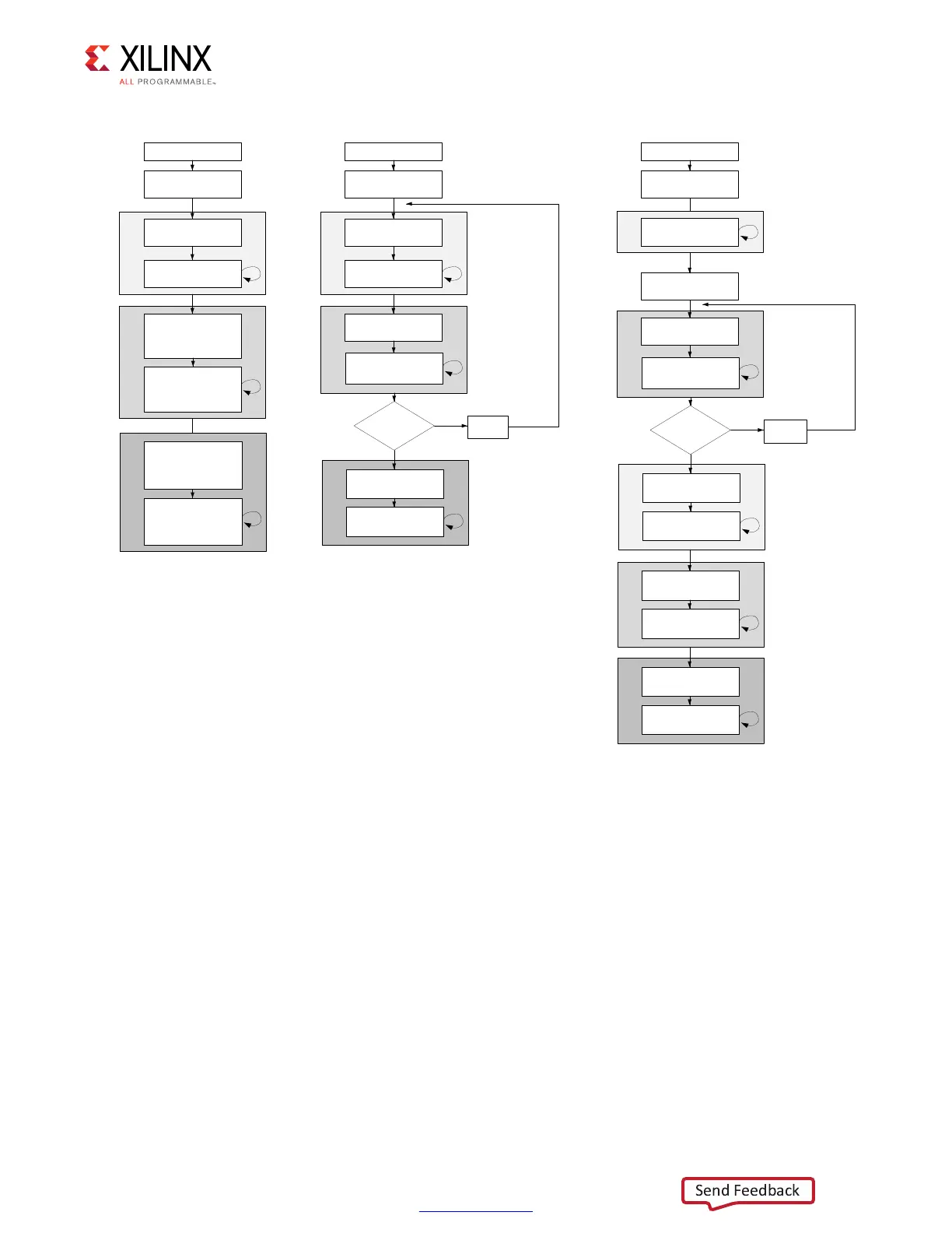
X-Ref Target - Figure 3-52
Figure 3-52: Calibration Flow Diagram
Write
A-5-0-F
or
A-5-0-F-9-6-D-2
Read
A-5-0-F
or
A-5-0-F-9-6-D-2
Reset
Memory Initialization
Write
0-F-0-F-0-F-F-0
Read
0-F-0-F-0-F-F-0
Stage 1:
Read Leveling
Stage 2:
Edge Advance Cal
Stage 2:
Rd Valid Cal
Simulation
RLDRAM II
Recalibrate read path
at each write
adjustment
Different pattern
from RTR
Write
A-5-0-F-3-C-3-C
or
A-5-0-F-9-6-D-2
Read
A-5-0-F
or
A-5-0-F-9-6-D-2
Write
A-5-0-F
Read
A-5-0-F
Reset
Memory Initialization
Write
0-F-0-F-0-F-F-0
Read
0-F-0-F-0-F-F-0
Stage 1:
Read Leveling
Stage 2:
Edge Advance Cal
Stage 2:
Rd Valid Cal
Write
A-5-0-F-3-C-3-C
Read
A-5-0-F
Write Cal
Done?
Adjust
Write Path
RLDRAM III
Writes not needed to
calibrate read path
Write
A-5-0-F-9-6-D-2
Read
A-5-0-F-9-6-D-2
Reset
Memory Initialization
Stage 1:
Read Leveling (RTR)
Stage 2:
Edge Advance Cal
Stage 1:
Read Leveling
Write
0-F-0-F-0-F-F-0
Read
0-F-0-F-0-F-F-0
Write Cal
Done?
Adjust
Write Path
Read
F-0-F-0-F-0-F-0
Turn Off Read Training
Register
Stage 2:
Edge Advance Cal
Write
A-5-0-F-9-6-D-2
Read
A-5-0-F-9-6-D-2
Stage 2:
Rd Valid Cal
Write
A-5-0-F-9-6-D-2
Read
A-5-0-F-9-6-D-2
 Loading...


