Zynq-7000 AP SoC and 7 Series FPGAs MIS v4.1 337
UG586 November 30, 2016
www.xilinx.com
Chapter 2: QDR II+ Memory Interface Solution
Customizing the Core
The 7 series FPGAs QDR II+ SRAM interface solution is customizable to support several
configurations. The specific configuration is defined by Verilog parameters in the top-level
of the core. As per the OOC flow, none of the parameter values are passed down to the user
design RTL file from the example design top RTL file. So, any design related parameter
change is not reflected in the user design logic. The MIG tool should be used to regenerate
a design when parameters need to be changed. These parameters are summarized in
Table 2-12.
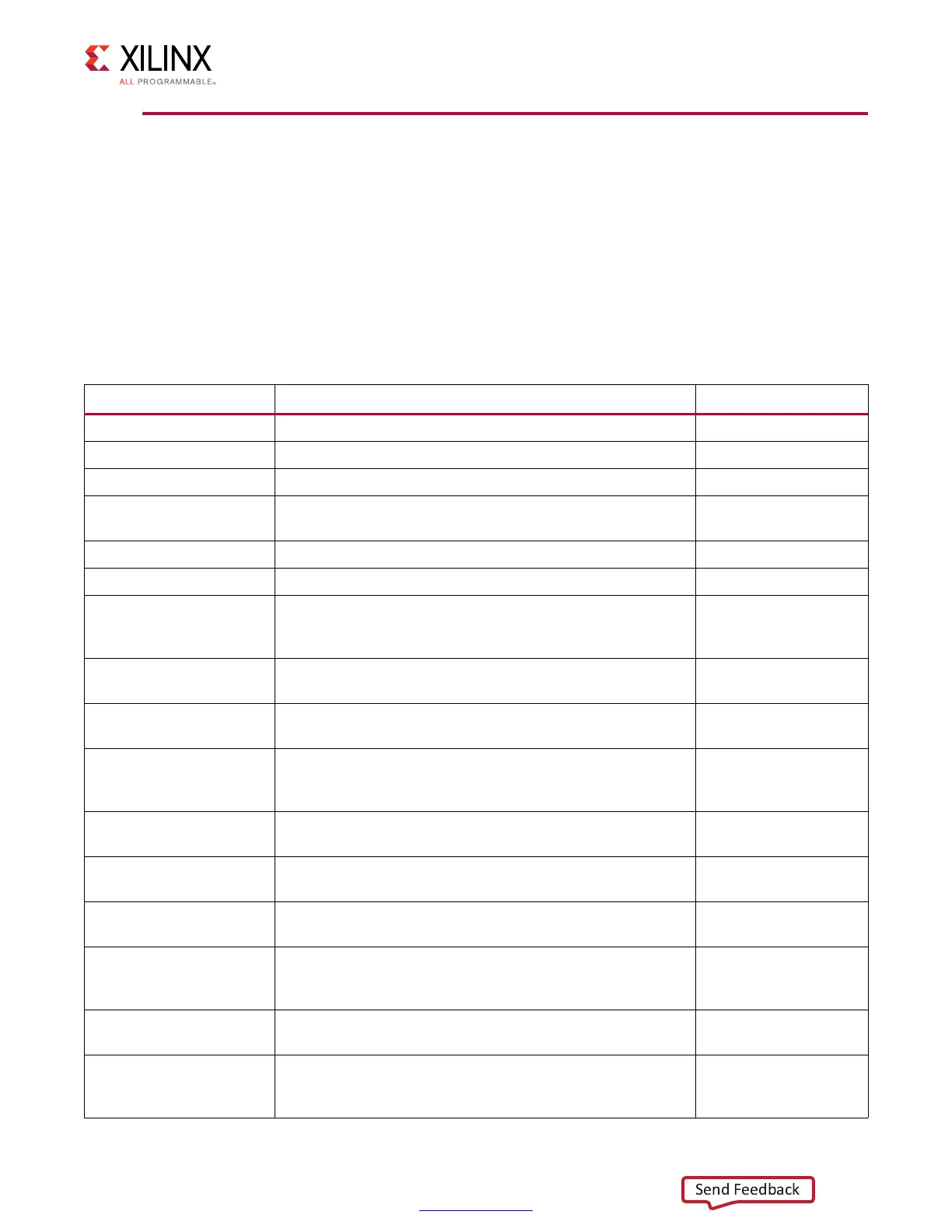
Table 2-12: 7 Series FPGAs QDR II+ SRAM Memory Interface Solution Configurable Parameters
Parameter Description Options
MEM_TYPE This is the memory address bus width QDR2PLUS
CLK_PERIOD This is the memory clock period (ps).
BURST_LEN This is the memory data burst length. 4
DATA_WIDTH
This is the memory data bus width and can be set through
the MIG tool. A maximum
DATA_WIDTH of 36 is supported.
BW_WIDTH This must be set to
DATA_WIDTH/9
NUM_DEVICES This is the number of memory devices used.
MEM_RD_LATENCY
This specifies the number of memory clock cycles of read
latency of the memory device used. This is derived from the
memory vendor data sheet.
2.0
2.5
FIXED_LATENCY_MODE
This indicates whether or not to use a predefined latency
for a read response from the memory to the client interface.
0, 1
CPT_CLK_CQ_ONLY
This indicates only one of the read clocks provided by the
memory (rise clock) is used for the data capture.
TRUE
PHY_LATENCY
This indicates the desired latency through the PHY for a
read from the time the read command is issued until the
read data is returned on the client interface.
CLK_STABLE
This is the number of cycles to wait until the echo clocks are
stable.
(See memory vendor
data sheet)
IODELAY_GRP
(1)
This is a unique name for the IODELAY_CTRL that is
provided when multiple IP cores are used in the design.
REFCLK_FREQ
This is the reference clock frequency for IDELAYCTRLs. This
parameter should not be changed.
200.0
RST_ACT_LOW
This is the active-Low or active-High reset. This is set to 1
when System Reset Polarity option is selected as active-Low
and set to 0 when the option is selected as active-High.
0, 1
IBUF_LPWR_MODE
This enables or disables low power mode for the input
buffers.
ON
OFF
IODELAY_HP_MODE
This enables or disables high-performance mode within the
IODELAY primitive. When set to OFF, the IODELAY operates
in low power mode at the expense of performance.
ON
OFF
 Loading...


