Zynq-7000 AP SoC and 7 Series FPGAs MIS v4.1 98
UG586 November 30, 2016
www.xilinx.com
Chapter 1: DDR3 and DDR2 SDRAM Memory Interface Solution
AXI4 Slave Interface Signals
Table 1-20 lists the AXI4 slave interface specific signal. All of the AXI interface signals are
synchronous to ui_clk.
C_S_AXI_HIGHADDR – Valid address
This parameter specifies the
high address for the memory
mapped slave interface. Address
requests received above this
value wrap back to the base
address. The base/high address
together define the accessible
size of the memory. This
accessible size must be a power
of two. Additionally, the
base/high address pair must be
aligned to a multiple of the
accessible size. The minimum
accessible size is 4,096 bytes.
C_S_AXI_PROTOCOL AXI4 AXI4
This parameter specifies the AXI
protocol.
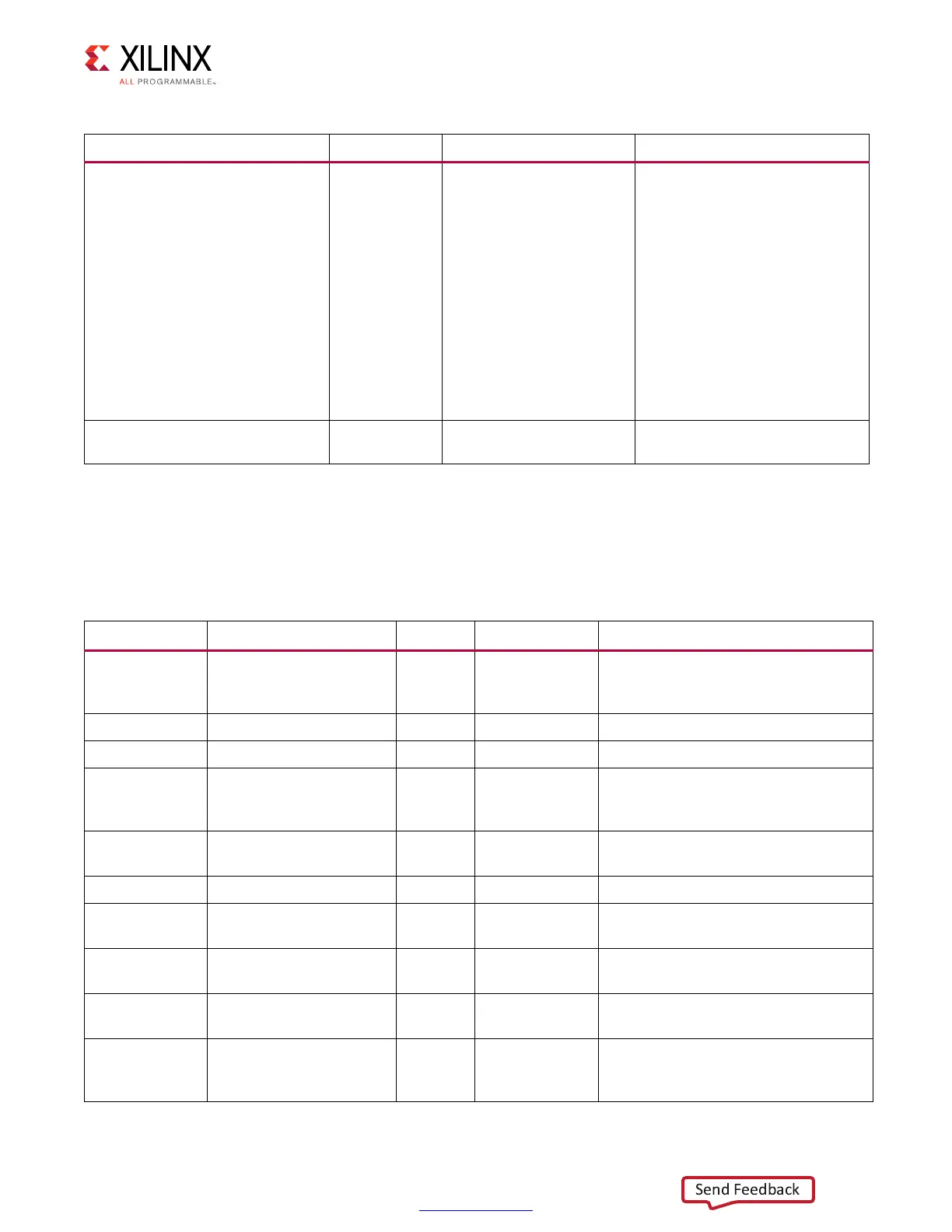
Table 1-19: AXI4 Slave Interface Parameters (Cont’d)
Parameter Name Default Value Allowable Values Description
Table 1-20: AXI4 Slave Interface Signals
Name Width Direction Active State Description
aresetn 1 Input Low
Input reset to the AXI Shim and it
should be in synchronous with FPGA
logic clock.
s_axi_awid C_AXI_ID_WIDTH Input Write address ID.
s_axi_awaddr C_AXI_ADDR_WIDTH Input Write address.
s_axi_awlen 8 Input
Burst length. The burst length gives
the exact number of transfers in a
burst.
s_axi_awsize 3 Input
Burst size. This signal indicates the
size of each transfer in the burst.
s_axi_awburst 2 Input Burst type.
s_axi_awlock 1 Input
Lock type. (This is not used in the
current implementation.)
s_axi_awcache 4 Input
Cache type. (This is not used in the
current implementation.)
s_axi_awprot 3 Input
Protection type. (Not used in the
current implementation.)
s_axi_awvalid 1 Input High
Write address valid. This signal
indicates that valid write address and
control information are available.
 Loading...


