Zynq-7000 AP SoC and 7 Series FPGAs MIS v4.1 414
UG586 November 30, 2016
www.xilinx.com
Chapter 3: RLDRAM II and RLDRAM 3 Memory Interface Solutions
user_design/rtl/ui
Table 3-5 lists the files in the user_design/rtl/ui directory.
user_design/rtl/phy
Table 3-6 lists the files in the user_design/rtl/phy directory.
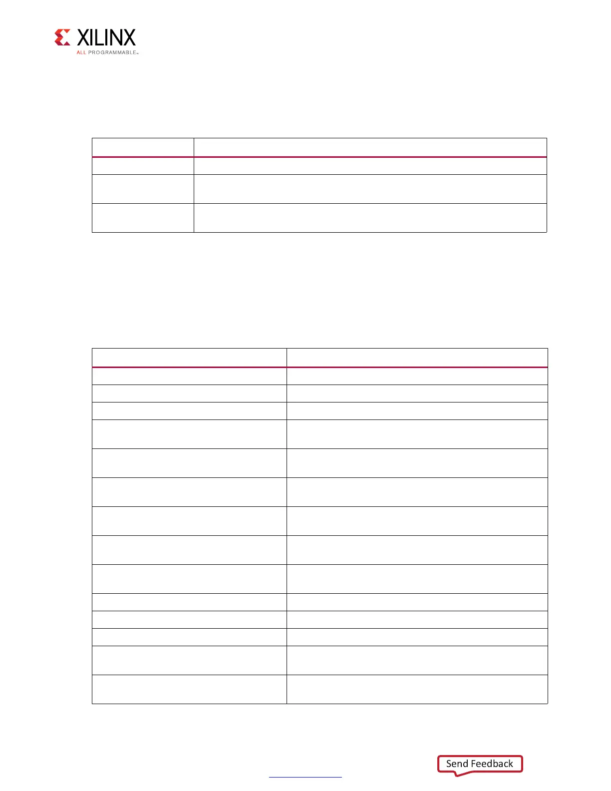
Table 3-5: Files in user_design/rtl/ui Directory
Name
(1)
Description
rld_ui_top.v This is the top-level wrapper for the user interface.
rld_ui_wr.v
This module generates the FIFOs used to buffer write data for the user
interface.
rld_ui_addr.v
This module generates the FIFOs used to buffer address and commands for the
user interface.
Notes:
1. All file names are prefixed with the MIG version number. For example, for the MIG 4.1 release module name of
rld_ui_top in generated output is now mig_7series_v4_1_rld_ui_top.
Table 3-6: Files in user_design/rtl/phy Directory
Name
(1)
Description
rld_phy_top.v This is the top-level module for the physical layer file.
rld_phy_write_top.v This is the top-level wrapper for the write path.
qdr_rld_phy_read_top.v This is the top-level of the read path.
qdr_rld_mc_phy.v
This module is a parameterizable wrapper instantiating
up to three I/O banks each with four-lane PHY primitives.
rld_phy_write_init_sm.v
This module contains the logic for the initialization state
machine.
rld_phy_write_control_io.v
This module contains the logic for the control signals
going to the memory.
rld_phy_write_data_io.v
This module contains the logic for the data and byte
writes going to the memory.
qdr_rld_prbs_gen.v
This PRBS module uses a many-to-one feedback
mechanism for 2n sequence generation.
qdr_rld_phy_ck_addr_cmd_delay.v
This module contains the logic to provide the required
delay on the address and control signals.
qdr_rld_phy_rdlvl.v This module contains the logic for stage 1 calibration.
qdr_rld_phy_read_stage2_cal.v This module contains the logic for stage 2 calibration.
qdr_rld_phy_read_data_align.v This module realigns the incoming data.
qdr_rld_phy_read_vld_gen.v
This module contains the logic to generate the valid
signal for the read data returned on the user interface.
rld_phy_byte_lane_map.v
This module handles the vector remapping between the
mc_phy module ports and the user memory ports.