Zynq-7000 AP SoC and 7 Series FPGAs MIS v4.1 115
UG586 November 30, 2016
www.xilinx.com
Chapter 1: DDR3 and DDR2 SDRAM Memory Interface Solution
The bank, row, and column comprise a target address on the memory device for read and
write operations. Commands are specified using the cmd[2:0] input to the core. The
available read and write commands are shown in Table 1-51.
accept
This signal indicates to the user design whether or not a request is accepted by the core.
When the accept signal is asserted, the request submitted on the last cycle is accepted, and
the user design can either continue to submit more requests or go idle. When the accept
signal is deasserted, the request submitted on the last cycle was not accepted and must be
retried.
use_addr
The user design asserts the use_addr signal to strobe the request that was submitted to
the native interface on the previous cycle.
data_buf_addr
The user design must contain a buffer for data used during read and write commands.
When a request is submitted to the native interface, the user design must designate a
location in the buffer for when the request is processed. For write commands,
data_buf_addr is an address in the buffer containing the source data to be written to the
external memory. For read commands, data_buf_addr is an address in the buffer that
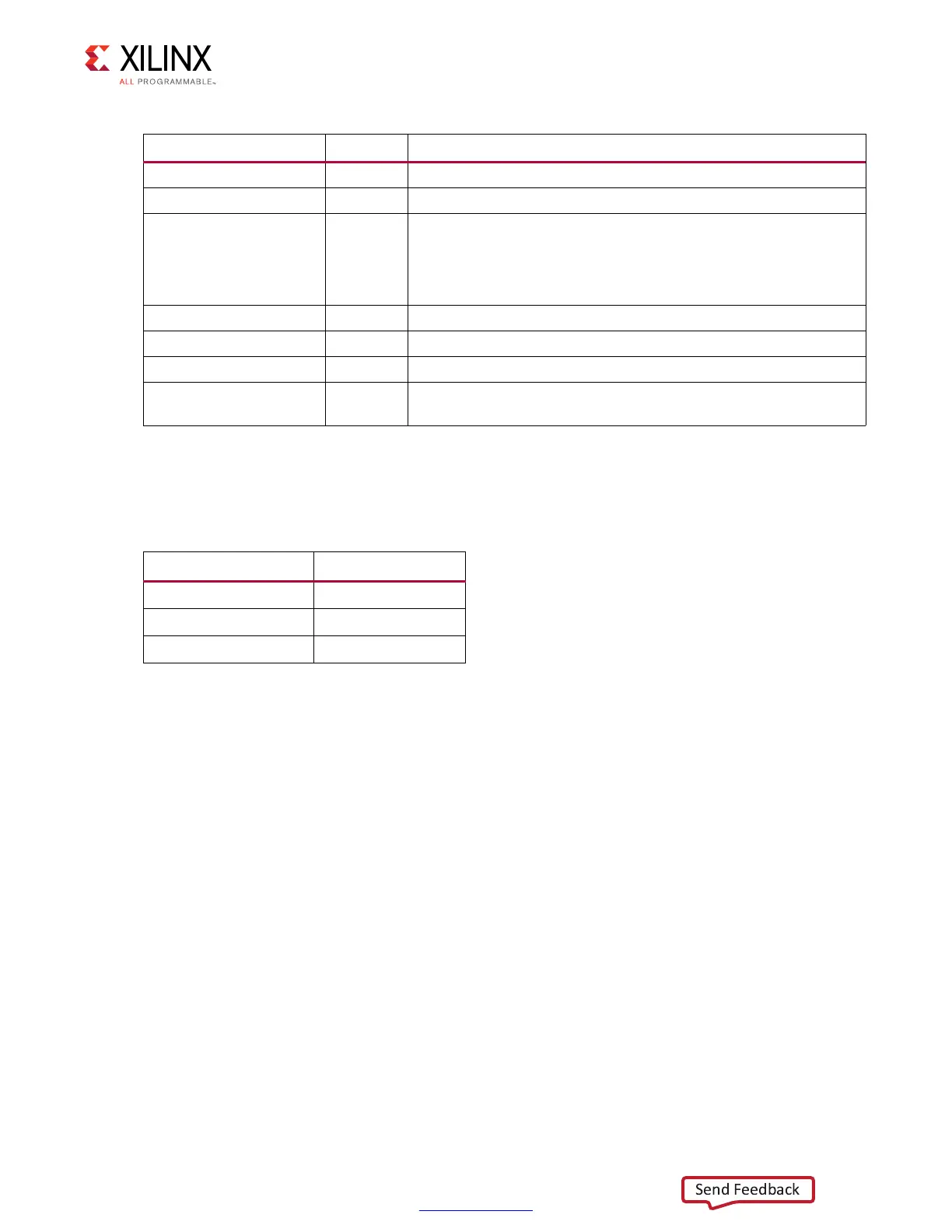
cmd[2:0] Input This input selects the command for the current request.
col[COL_WIDTH – 1:0] Input This input selects the column address for the current request.
data_buf_addr[7:0] Input
This input indicates the data buffer address where the Memory
Controller:
• Locates data while processing write commands.
• Places data while processing read commands.
hi_priority Input This input is reserved and should be connected to logic 0.
rank[] Input This input is reserved and should be connected to logic 0.
row[ROW_WIDTH – 1:0] Input This input selects the row address for the current request.
use_addr Input
The user design strobes this input to indicate that the request
information driven on the previous state is valid.
Table 1-51: Memory Interface Commands
Operation cmd[2:0] Code
Memory write 000
Memory read 001
Reserved All other codes
Table 1-50: Native Interface Command Signals (Cont’d)
Signal Direction Description