Zynq-7000 AP SoC and 7 Series FPGAs MIS v4.1 582
UG586 November 30, 2016
www.xilinx.com
Chapter 4: LPDDR2 SDRAM Memory Interface Solution
accept
This signal indicates to the user design whether or not a request is accepted by the core.
When the accept signal is asserted, the request submitted on the last cycle is accepted, and
the user design can either continue to submit more requests or go idle. When the accept
signal is deasserted, the request submitted on the last cycle was not accepted and must be
retried.
use_addr
The user design asserts the use_addr signal to strobe the request that was submitted to
the native interface on the previous cycle.
data_buf_addr
The user design must contain a buffer for data used during read and write commands.
When a request is submitted to the native interface, the user design must designate a
location in the buffer for when the request is processed. For write commands,
data_buf_addr is an address in the buffer containing the source data to be written to the
external memory. For read commands, data_buf_addr is an address in the buffer that
receives read data from the external memory. The core echoes this address back when the
requests are processed.
Write Command Signals
The native interface has signals that are used when the Memory Controller is processing a
write command (Table 4-18). These signals connect to the control, address, and data signals
of a buffer in the user design.
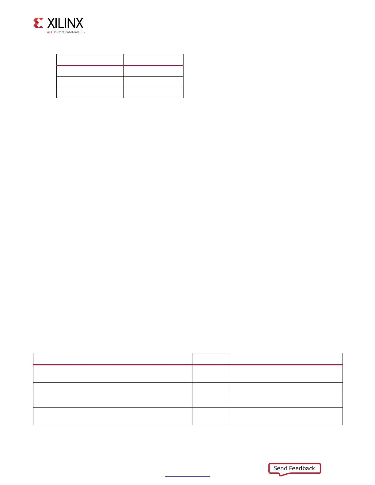
Table 4-17: Memory Interface Commands
Operation cmd[2:0] Code
Memory read 000
Memory write 001
Reserved All other codes
Table 4-18: Native Interface Write Command Signals
Signal Direction Description
wr_data[2 × nCK_PER_CLK × PAYLOAD_WIDTH – 1:0] Input
This is the input data for write
commands.
wr_data_addr [DATA_BUF_ADDR_WIDTH – 1:0] Output
This output provides the base address
for the source data buffer for write
commands.
wr_data_mask[2 × nCK_PER_CLK × DATA_WIDTH/8 – 1:0] Input
This input provides the byte enable for
the write data.
 Loading...


