Zynq-7000 AP SoC and 7 Series FPGAs MIS v4.1 595
UG586 November 30, 2016
www.xilinx.com
Chapter 4: LPDDR2 SDRAM Memory Interface Solution
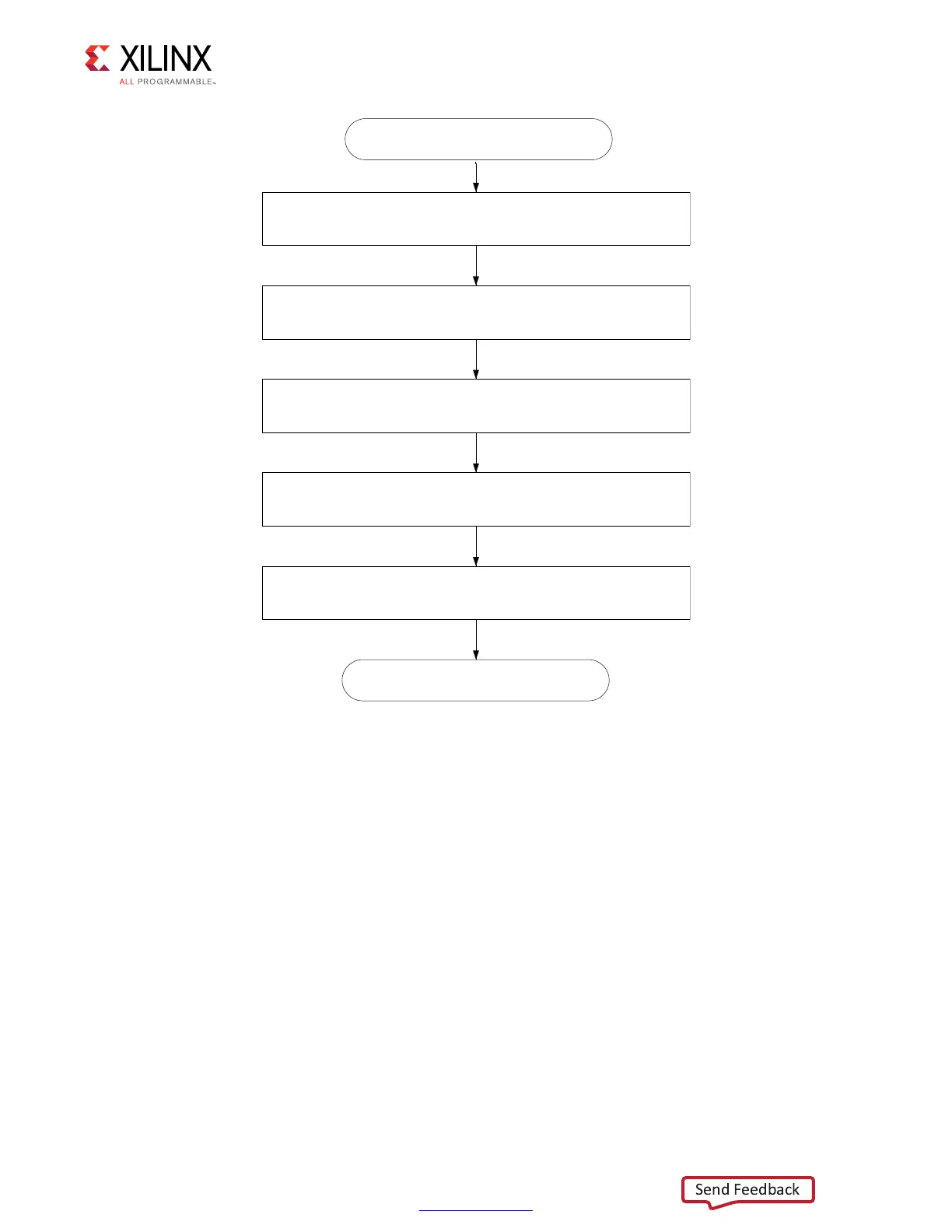
The calibration stages in Figure 4-49 correspond to these sections:
• Memory Initialization, page 604
• Read Leveling, page 604
• Read Valid Calibration, page 607
• PRBS Read Leveling, page 607
• Phase Detector, page 608
I/O Architecture
Each 7 series FPGA I/O bank has dedicated blocks comprising a PHY control block, four
PHASER_IN and PHASER_OUT blocks, four IN/OUT_FIFOs, ISERDES, OSERDES, ODDR,
IDELAY, and IOBs. A single PHY control block communicates with all four PHASER_IN and
PHASER_OUT blocks within the I/O bank.
X-Ref Target - Figure 4-49
Figure 4-49: PHY Overall Initialization and Calibration Sequence
System Reset
PHY Initialization and Calibration Complete
LPDDR2 SDRAM initialization
Read leveling stage1 calibration with static data of FF,00,FF,00,FF,00,FF,00
Read Valid calibration to generate rd_valid aligned with read data from SDRAM
PRBS Read leveling ( Read DQS centering in read DQ window with PRBS pattern to
account for ISI effects)
Phase Detector calibration ( Calibrate to set trigger points to compensate for Drift due
to voltage and temperature changes)
 Loading...


