Zynq-7000 AP SoC and 7 Series FPGAs MIS v4.1 376
UG586 November 30, 2016
www.xilinx.com
Chapter 2: QDR II+ Memory Interface Solution
Read Stage 2 Calibration Debug
Table 2-21 indicates the mapping between bits within the dbg_rd_stage2_cal bus and
debug signals in the PHY. All signals are found within the
qdr_rld_phy_read_stage2_cal module and are all valid in the clk domain.
dbg_rd_stage1_cal[109] samp_result_held_r Result from previous sample cycle.
dbg_rd_stage1_cal[154+:40] simp_dlyval_r Five bits per lane dlyval results for simple pattern.
dbg_rd_stage1_cal[194+:48] simp_left_r Six bits per lane left results for simple pattern.
dbg_rd_stage1_cal[194+:48] simp_right_r Six bits per lane right results for simple pattern.
dbg_rd_stage1_cal[194+:48] simp_center_r Six bits per lane center results for simple pattern.
dbg_rd_stage1_cal[378+:48] cmplx_left_r Six bits per lane left results for complex pattern.
dbg_rd_stage1_cal[426+:48] cmplx_right_r Six bits per lane right results for complex pattern.
dbg_rd_stage1_cal[474+:48] cmplx_center_r Six bits per lane center results for complex pattern.
dbg_rd_stage1_cal[682+:48] simp_left_63
Left edge result is 63 for simple pattern, one bit per
lane.
dbg_rd_stage1_cal[690+:48] cmplx_left_63
Left edge result is 63 for complex pattern, one bit per
lane.
dbg_rd_stage1_cal[698+:48] simp_right_63
Right edge result is 63 for simple pattern, one bit per
lane.
dbg_rd_stage1_cal[706+:48] cmplx_right_63
Right edge result is 63 for complex pattern, one bit per
lane.
dbg_rd_stage1_cal[522+:72] rd_data_lane_r
Aligned PHY data for lane currently undergoing
calibration.
dbg_rd_stage1_cal[594+:72] iserdes_lane_r Raw PHY data for lane currently undergoing calibration.
dbg_rd_stage1_cal[714+:72] cmplx_rd_burst_bytes Complex data to compare against memory read data.
dbg_rd_stage1_cal[786+:9] bit_comp Cumulative compare per bit.
dbg_rd_stage1_cal[795+:8] simp_min_eye_r Minimum eye detected per lane simple pattern.
dbg_rd_stage1_cal[803+:8] cmplx_min_eye_r Minimum eye detected per lane complex pattern.
Table 2-20: Read Stage 1 Debug Signal Map (Cont’d)
Bits PHY Signal Name Description
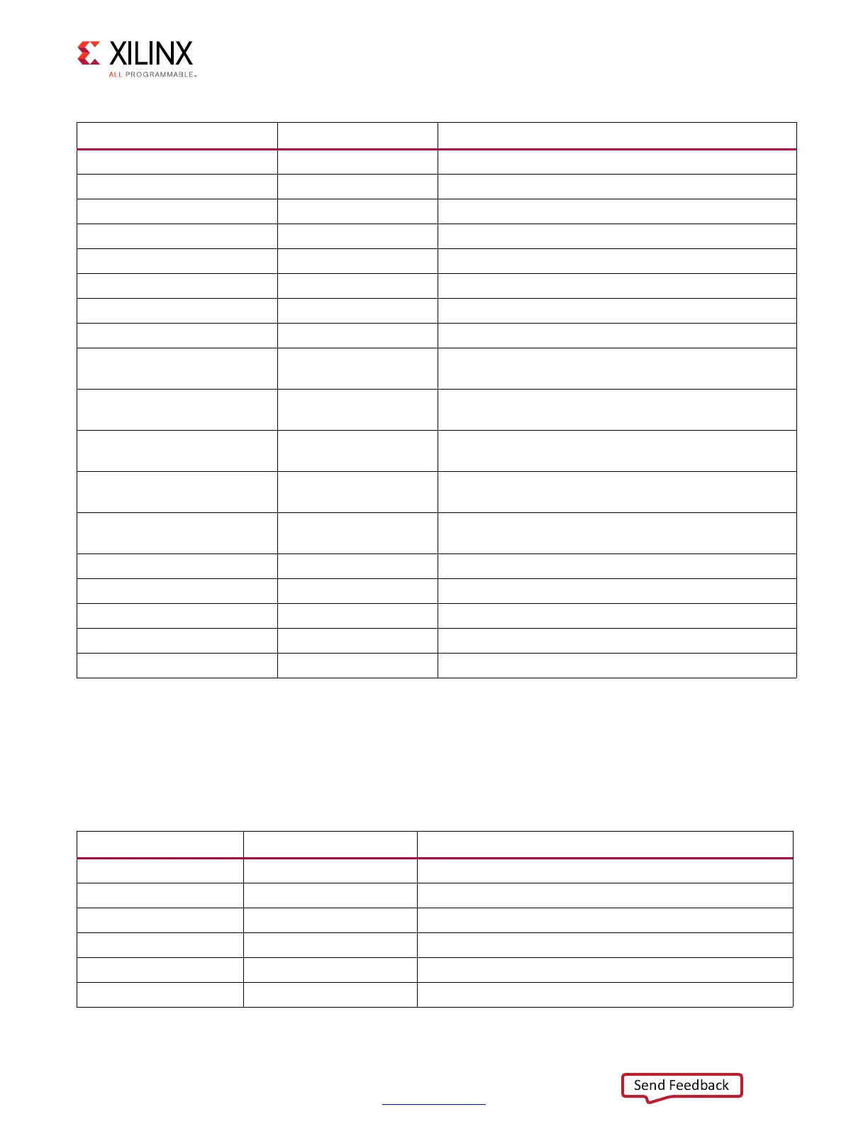
Table 2-21: Read Stage 2 Debug Signal Map
Bits PHY Signal Name Description
dbg_stage2_cal[0] en_mem_latency Signal to enable latency measurement
dbg_stage2_cal[5:1] latency_cntr[0] Indicates the latency for the first byte lane in the interface
dbg_stage2_cal[6] rd_cmd Internal rd_cmd for latency calibration
dbg_stage2_cal[7] latency_measured[0] Indicates latency has been measured for byte lane 0
dbg_stage2_cal[8] bl4_rd_cmd_int Indicates calibrating for burst length of 4 data words
dbg_stage2_cal[9] bl4_rd_cmd_int_r Internal register stage for burst 4 read command