Zynq-7000 AP SoC and 7 Series FPGAs MIS v4.1 149
UG586 November 30, 2016
www.xilinx.com
Chapter 1: DDR3 and DDR2 SDRAM Memory Interface Solution
Multi-Purpose Register Read Leveling
At this stage of calibration, the write DQS is not centered in the write DQ window nor is the
read DQS centered in the read DQ window. The Multi-Purpose Register (MPR) is used to
center the read DQS in the read DQ window. The MPR has a predefined 01010101 pattern
that is read back during this stage of calibration. Read DQS centering is required for the next
stage of calibration.
MPR read leveling is performed on a per byte basis and it is a two step process.
• The first step is to delay all the DQ bits in a byte using IDELAY taps by monitoring Bit[0]
in that byte. The DQ bits are moved to place the first valid rising edge data after the
first rising edge of DQS.
• The second step is to sweep DQS across the entire byte window using PHASER_IN fine
taps to detect two edges. The entire DQ byte lane (Bits[7:0]) is monitored while
sweeping the byte window to find the aggregate eye. Note that although the JEDEC
standard states it is only required to send the MPR pattern on Bit[0] of a byte, all
vendors tested sent the MPR pattern on the entire byte.
• Minimum data window (MIN_EYE_SIZE) must be met for two edges to be found.
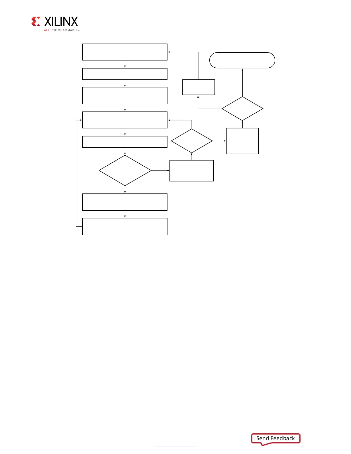
X-Ref Target - Figure 1-65
Figure 1-65: Write Leveling Flow Diagram
5'?C??
.O
.O
.O
9E S
)SCURRENT
RANKDONE
)NCREMENT$13
COUNTTONEXT$13
INACTIVERANK
)SSUE-2TO
$ISABLE7RITE
,EVELFOR
#URRENT2ANK
)NCREMENT
2ANK#OUNT
$EASSERT7RITE?CALIB?N
)NPUTTO0HASER#ONTROL"LOCK
)SSUE-2#OMMANDTO%NABLE
72,6,FOR#URRENT2ANK
!SSERTWRITE?CALIB?N)NPUTTO0(9
#ONTROL"LOCKAFTER7,$13%.
9E S
9E S
)SSUE7RITE#OMMANDTO0(9
#ONTROL"LOCKFOR$130ULSE'ENERATION
)NCREMENT&INE#OARSE0(!3%2?/54
$ELAYFOR$13BEING7RITE,EVELED
7AITA&EW#YCLESFOR0(!3%2?/54
$ELAYTO3ETTLE
!SSERT/$4AFTER-/$
7AITFOR-EMORY#LOCK#YCLES
!LL2ANKS
$ONE
TO
4RANSITION7HEN
3TABLE#OUNTER
 Loading...


