Zynq-7000 AP SoC and 7 Series FPGAs MIS v4.1 617
UG586 November 30, 2016
www.xilinx.com
Chapter 4: LPDDR2 SDRAM Memory Interface Solution
The app_wdf_end signal must be used to indicate the end of a memory write burst. For
memory burst types of eight, the app_wdf_end signal must be asserted on the second
write data word.
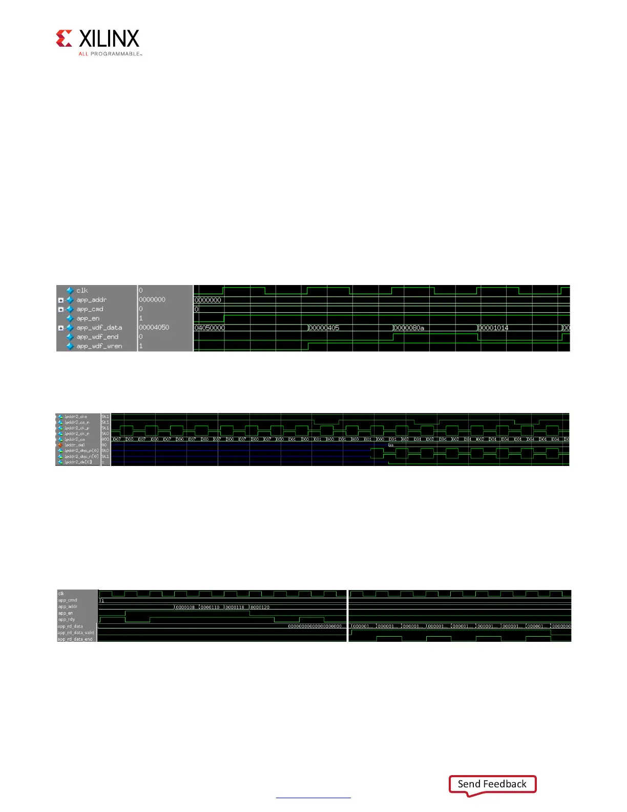
The map of the application interface data to the DRAM output data can be explained with
an example.
For a 2:1 Memory Controller, the User Interface clock to DRAM clock ratio is 2:1. For an 8-bit
wide memory interface, the User Interface data width is 32-bit wide (8 × 2 × 2 =
mem_data_width × nck_per_clk × ddr_rate). To perform a BL8 transaction, write data
at the application interface must be provided in two clock cycles. The app_wdf_end signal
is asserted for the second data as shown in Figure 4-62. In this case, the application data
provided in the first cycle is 0000_0405 (Hex), and the data provided in the last cycle is
0000_080A (Hex). This is for a BL8 transaction.
Figure 4-63 shows the corresponding data at the DRAM interface.
Read Path
The read data is returned by the UI in the requested order and is valid when
app_rd_data_valid is asserted (Figure 4-64 and Figure 4-65). The app_rd_data_end
signal indicates the end of each read command burst.
X-Ref Target - Figure 4-62
Figure 4-62: Data at the Application Interface for 2:1 Mode
X-Ref Target - Figure 4-63
Figure 4-63: Data at the DRAM Interface for 2:1 Mode
X-Ref Target - Figure 4-64
Figure 4-64: UI Interface Read Timing Diagram (Memory Burst Type = BL8)