Zynq-7000 AP SoC and 7 Series FPGAs MIS v4.1 251
UG586 November 30, 2016
www.xilinx.com
Chapter 1: DDR3 and DDR2 SDRAM Memory Interface Solution
The MIG design only looks at DQ[0]. If there is an issue with DQ[0], the MPR calibration
stage would fail.
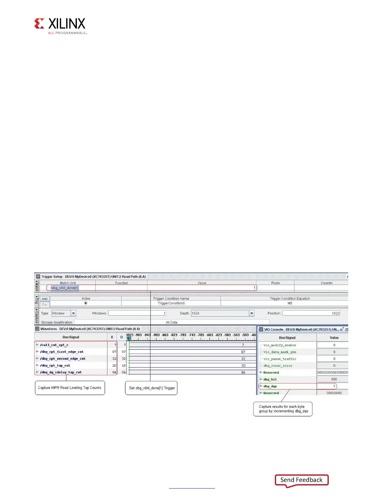
•If a DQS byte group failed this stage of calibration, cal1_cnt_cpt_r would equal the
byte number that is failing as no further progress or increment on cal1_cnt_cpt_r
occurred.
• Check if the failing DQS byte has an dq_idelay_tap_cnt value of 31. This means the
algorithm ran out of taps searching for the capture edges.
•Check and compare the dq_idelay_tap_cnt, cpt_first_edge_cnt,
cpt_second_edge_cnt, and cpt_tap_cnt values across bytes during MPR read
leveling.
• Look at idelay_tap_cnt for each byte group. The idelay_tap_cnt across the DQS
byte groups should only vary by 2 to 3 taps
• Look at how many edges (up to two) were found. Less than two edges can be found
when running around or below 400 MHz. Otherwise, two edges should always be
found.
• Using high quality probes and scope, probe the address/command to ensure the load
register command to the DRAM that enables MPR was correct. To enable the MPR, a
MODE Register Set (MRS) command is issued to the MR3 Register with bit A2 = 1. To
make this measurement, bring mpr_rdlvl_start to an I/O pin and use as the trigger
to capture A2 (must be 1) and WE_N (must be 0).
Expected Vivado Logic Analyzer Tool Results
X-Ref Target - Figure 1-102
Figure 1-102: Trigger = dbg_rdlvl_done[1]