Zynq-7000 AP SoC and 7 Series FPGAs MIS v4.1 350
UG586 November 30, 2016
www.xilinx.com
Chapter 2: QDR II+ Memory Interface Solution
c. The differential signals at the input pins meet the VIDIFF (min) requirements in the
corresponding LVDS or LVDS_25 DC specifications tables of the specific device
family data sheet.
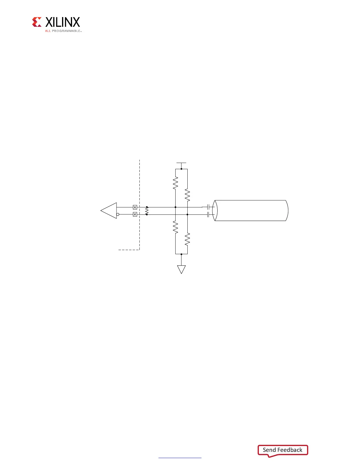
One way to accomplish the above criteria is to use an external circuit that both
AC-couples and DC-biases the input signals. The figure shows an example circuit for
providing an AC-coupled and DC-biased circuit for a differential clock input. RDIFF
provides the 100Ω differential receiver termination because the internal DIFF_TERM
is set to FALSE. To maximize the input noise margin, all RBIAS resistors should be the
same value, essentially creating a VICM level of VCCO/2. Resistors in the 10k to
100 kΩ range are recommended. The typical values for the AC coupling capacitors
CAC are in the range of 100 nF. All components should be placed physically close to
the FPGA inputs.
Note:
The last set of guidelines on differential LVDS inputs are added within the LVDS and LVDS_25
(Low Voltage Differential Signaling) section of the 7 Series SelectIO Resources User Guide (UG471)
[Ref 2] in the next release of the document.
These guidelines are irrespective of Package, Column (HR/HP), or I/O Voltage.
Sharing sys_clk between Controllers
The MIG 7 series FPGA designs require sys_clk to be in the same I/O bank column as the
memory interface to minimize jitter.
• Interfaces Spanning I/O Columns – A single sys_clk input cannot drive memory
interfaces spanning multiple I/O columns. The input clock input must be in the same
column as the memory interface to drive the PLL using the CMT Backbone, which
minimizes jitter.
• Interfaces in Single I/O Column – If the memory interfaces are entirely contained
within the same I/O column, a common sys_clk can be shared among the interfaces.
X-Ref Target - Figure 2-47
Figure 2-47: Example Circuit for AC-Coupled and DC-Biased Differential Clock Input
C
AC
R
DIFF
= 100Ω
C
AC
Differential Transmission Line
R
BIAS
R
BIAS
R
BIAS
R
BIAS
P
N
V
CCO
FPGA
Differential Clock
Input to the FPGA
LVDS or
LVDS_25
Input Buffer
 Loading...


