Zynq-7000 AP SoC and 7 Series FPGAs MIS v4.1 146
UG586 November 30, 2016
www.xilinx.com
Chapter 1: DDR3 and DDR2 SDRAM Memory Interface Solution
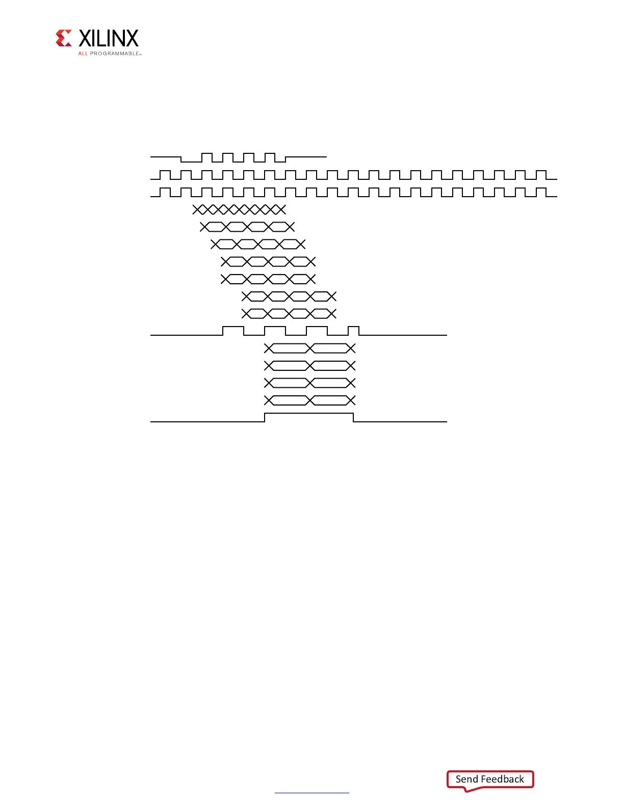
Each byte group can be read out of the IN_FIFO on different PHY_Clk cycles due to fly-by
routing and delay differences within each group. Therefore, the IN_FIFO Not Empty flags for
all the byte groups are ANDed together and used as the read enable for all data IN_FIFOs.
Figure 1-61 shows the read data capture timing diagram.
Write Leveling
Write leveling, which is a feature available in DDR3 SDRAM, is performed in this stage of
calibration. DDR3 SDRAM modules have adopted fly-by topology on clocks, address,
commands, and control signals to improve signal integrity. Specifically, the clocks, address,
and control signals are all routed in a daisy-chained fashion, and termination is located at
the end of each trace. However, this causes a skew between the strobe (DQS) and the clock
(CK) at each memory device on the module. Write leveling, a new feature in DDR3 SDRAMs,
allows the controller to adjust each write DQS phase independently with respect to the CK
forwarded to the DDR3 SDRAM device. This compensates for the skew between DQS and CK
and meets the t
DQSS
specification.
During write leveling, DQS is driven by the FPGA memory interface and DQ is driven by the
DDR3 SDRAM device to provide feedback. The FPGA memory interface has the capability to
delay DQS until a 0-to-1 transition is detected on DQ. Write leveling is performed once after
power-up. The calibration logic ORs the DQ bits in a byte to determine the transition
because different memory vendors use different bits in a byte as feedback. The DQS delay
can be achieved with the PHASER_OUT fine and coarse delay adjustment in the 7 series
FPGAs. Figure 1-62 shows the write leveling block diagram.
X-Ref Target - Figure 1-61
Figure 1-61: Read Data Capture Timing Diagram
5'?C??
$13#ENTEREDIN
6ALID$ATA7INDOW
2D"#,+
1)NPUT
1)NPUT
1)NPUT
1)NPUT
)3%2$%31/UTPUT
)3%2$%31/UTPUT
)3%2$%31/UTPUT
)3%2$%31/UTPUT
).?&)&/WR?%NABLE
2D$IV"#,+
 Loading...


