Zynq-7000 AP SoC and 7 Series FPGAs MIS v4.1 602
UG586 November 30, 2016
www.xilinx.com
Chapter 4: LPDDR2 SDRAM Memory Interface Solution
Datapath
The datapath comprises the write and read datapaths. The datapath in the 7 series FPGA is
completely implemented in dedicated logic with IN/OUT_FIFOs interfacing the FPGA logic.
The IN/OUT_FIFOs provide datapath serialization/deserialization in addition to clock
domain crossing, thereby allowing the FPGA logic to operate at low frequencies up to 1/2
the frequency of the LPDDR2 SDRAM clock. Figure 4-52 shows the block diagram of the
datapath.
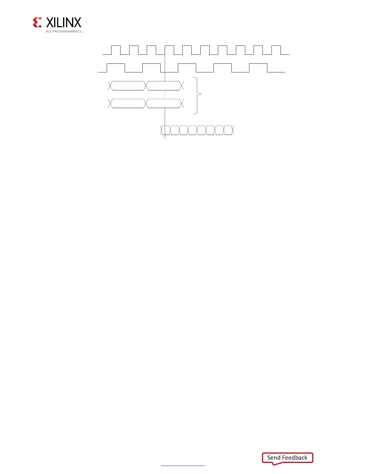
X-Ref Target - Figure 4-51
Figure 4-51: Address/Command Timing Diagram
{Cmd1F,cmd1R}
{Cmd2F,cmd2R}
{Cmd3F,cmd3R}
{Cmd4F,cmd4R}
Inputs to OSERDES in DDR mode
C1R
C1
F
C2R C2F C3R
C3F
C4R
C4F
OSERDES Output for
CA
CLK
CLKDIV2
CA, CS_N
 Loading...


