Zynq-7000 AP SoC and 7 Series FPGAs MIS v4.1 260
UG586 November 30, 2016
www.xilinx.com
Chapter 1: DDR3 and DDR2 SDRAM Memory Interface Solution
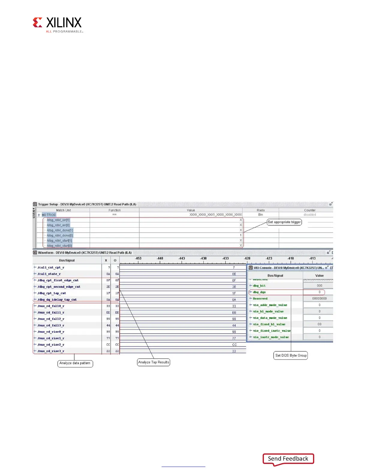
• Look at how many edges (up to two) were found. Less than two edges can be found
when running around or below 400 MHz. Otherwise, two edges should always be found
to then center the IDELAY taps.
• Determine if any bytes completed successfully. The read leveling algorithm sequentially
steps through each DQS byte group detecting the capture edges. When the failure
occurs, the value on cal1_cnt_cpt_r indicates the byte that failed edge detection.
• If the incorrect data pattern is detected, determine if the error is due to the write access
or the read access. See the Determining If a Data Error is Due to the Write or Read
section.
•If the dbg_rdlvl_err[0] is asserted (read leveling failure), use high quality probes
and scope observe the DQS-to-DQ phase relationship during a write. The scope trigger
should be dbg_rdlvl_start[0]. The alignment should be approximately 90°.
• If the DQS-to-DQ alignment is correct, observe the WE_N-to-DQS relationship to see if
it meets CWL again using dbg_rdlvl_start[0] as a trigger.
Expected Vivado Logic Analyzer Tool Results
X-Ref Target - Figure 1-105
Figure 1-105: Trigger = dbg_rdlvl_done[0]