Zynq-7000 AP SoC and 7 Series FPGAs MIS v4.1 502
UG586 November 30, 2016
www.xilinx.com
Chapter 3: RLDRAM II and RLDRAM 3 Memory Interface Solutions
The read calibration results are provided as part of the Debug port as various output
signals. These signals can be used to capture and evaluate the read calibration results.
Read calibration uses the IODELAY to align the capture clock in the data valid window for
captured data. The algorithm shifts the IDELAY/PHASER_IN values and looks for edges of
the data valid window on a per-byte basis as part of the calibration procedure.
DEBUG_PORT Signals
The top-level wrapper, user_top, provides several output signals that can be used to
debug the core if the debug option is checked when generating the design through the MIG
tool. Each debug signal output begins with dbg_. The DEBUG_PORT parameter is always set
to OFF in the sim_tb_top module of the sim folder, which disables the debug option for
functional simulations. These signals and their associated data are described in Table 3-28.
dbg_phy_status[11] edge_adv_cal_start
Edge Advance calibration start
signal
N/A
dbg_phy_status[12] edge_adv_cal_done
Edge Advance calibration is
complete
Make sure the expected data is
being returned from the
memory. Check results of stage
1 read calibration. Check the
results of write calibration (if
enabled).
dbg_phy_status[13] init_cal_done Latency calibration completed
Check which byte lane failed
and check the margin found
during read training stage 1 and
write calibration for the byte
lane that fails.
dbg_phy_status[14] init_calib_complete Calibration complete N/A
Notes:
1. N/A indicates that as long as previous stages have completed, this stage is also completed.
Table 3-27: Physical Layer Simple Status Bus Description Defined in the rld_phy_top Module (Cont’d)
Debug Port Signal Name Description If Problems Arise
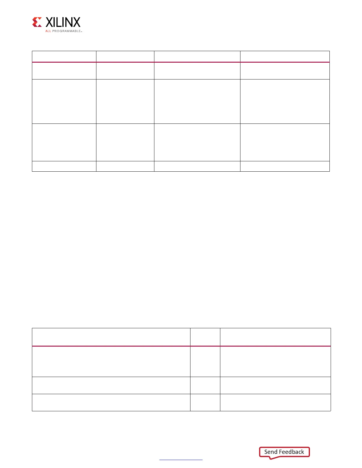
Table 3-28: DEBUG_PORT Signal Descriptions
Signal Direction Description
dbg_phy_cmd_n[nCK_PER_CLK × 3 – 1:0] Output
This active-Low signal is the internal
command that is sent to the memory
used for debug with the Vivado logic
analyzer feature.
dbg_phy_addr[nCK_PER_CLK × RLD_ADDR_WIDTH × 2 –
1:0]
Output
Address being accessed for the
commands given with dbg_phy_cmd_n.
dbg_phy_ba[nCK_PER_CLK × BANK_WIDTH × 2 – 1:0] Output
Control bank address bus used for debug
with the Vivado logic analyzer feature.
 Loading...


